Semiconductor process

a technology of semiconductors and process steps, applied in the direction of semiconductor/solid-state device manufacturing, basic electric elements, electric devices, etc., can solve the problems of increasing the complexity of the design of ics, and achieve the effect of ensuring device reliability and yield, and improving the accuracy of pattern transfer

Inactive Publication Date: 2013-02-21
UNITED MICROELECTRONICS CORP
View PDF7 Cites 0 Cited by
  • Summary
  • Abstract
  • Description
  • Claims
  • Application Information

AI Technical Summary

Benefits of technology

[0006]Accordingly, the present invention is directed to a semiconductor process, so as to improve accuracy of the pattern transferring and thereby ensure the device reliability and yield.

Problems solved by technology

As the devices are continuously miniaturized and integrated, the design of the ICs becomes increasingly complicated, such that accuracy of the pattern transferring is quite important.

Method used


Image

  • Semiconductor process
  • Semiconductor process
  • Semiconductor process

Examples


Embodiment Construction

[0024]Reference will now be made in detail to the present preferred embodiments of the invention, examples of which are illustrated in the accompanying drawings. Wherever possible, the same reference numbers are used in the drawings and the description to refer to the same or like parts.

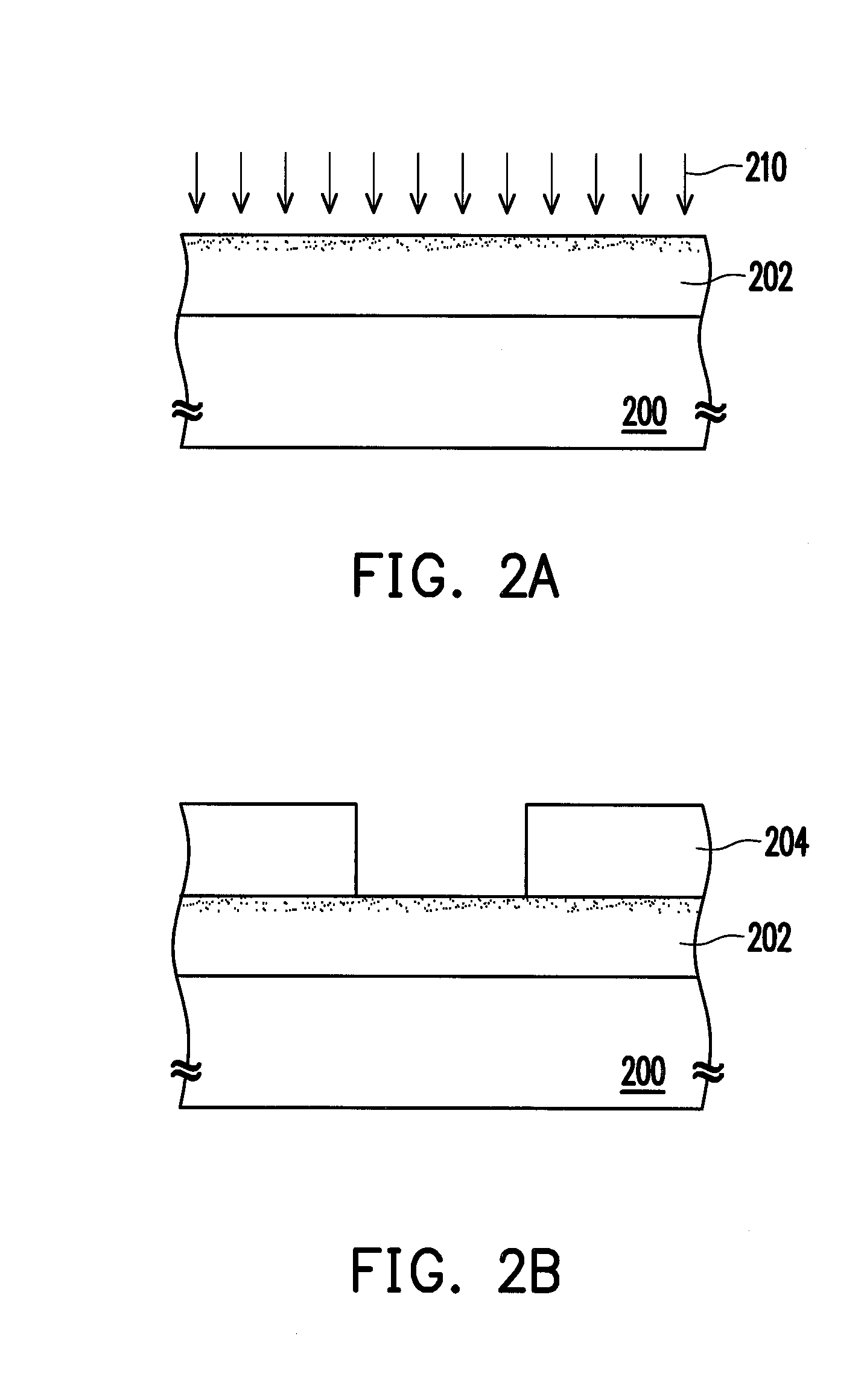
[0025]FIG. 1 is a flow chart illustrating a semiconductor process according to a first embodiment of the present invention. FIGS. 2A-2B depict, in a cross-sectional view, a semiconductor process according to a first embodiment of the present invention.

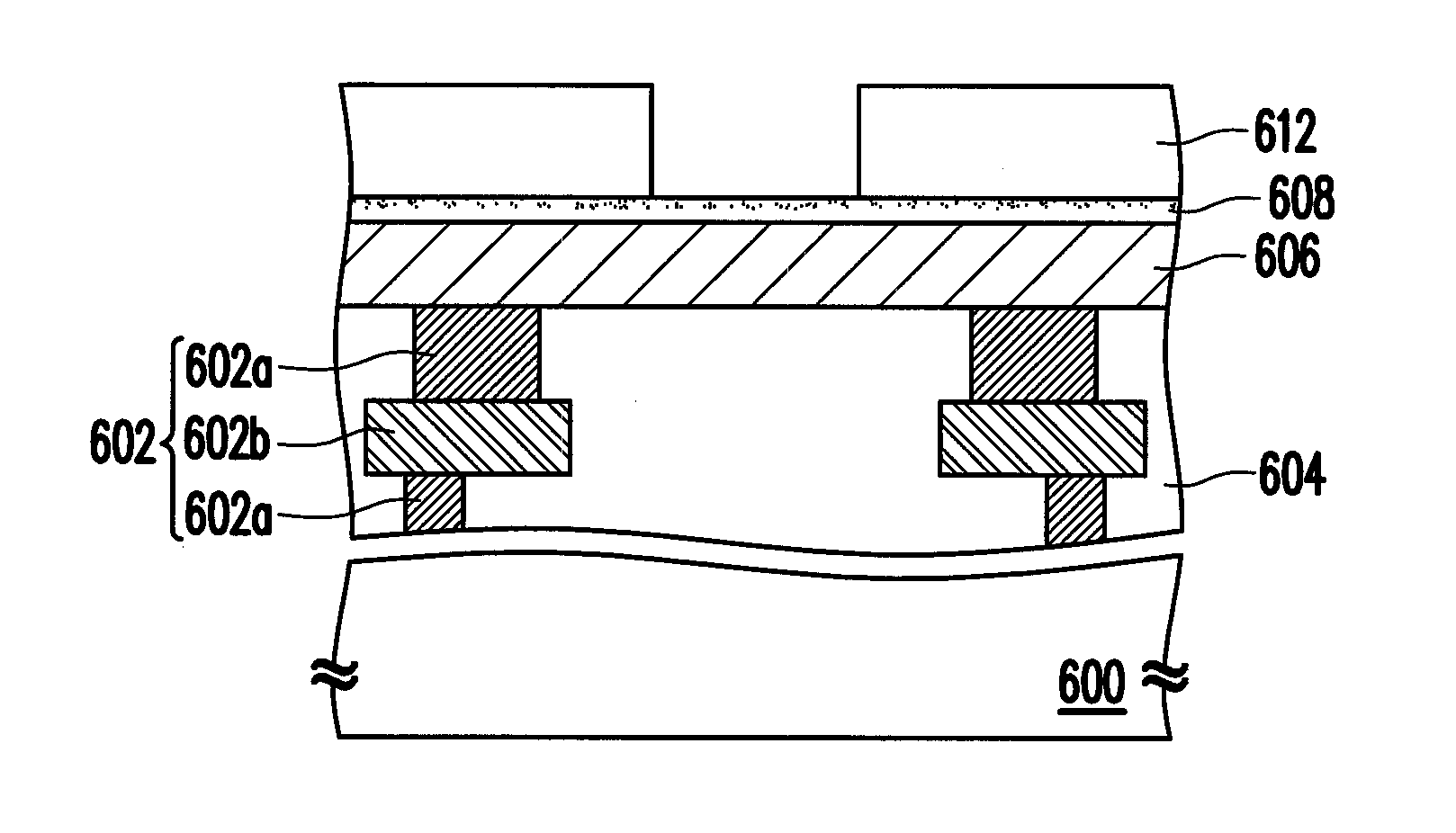
[0026]Referring to FIGS. 1 and 2A, in step S102, a substrate 200 is provided, and a material layer 202 is then formed on the substrate 200. The substrate 200 can be a semiconductor wafer, e.g. an N- or a P-type silicon wafer, whereon thin films, conductive parts, or even semiconductor devices may be formed. It is mentionable that the material layer 202 can be a barrier layer or a conductive layer in an interconnection structure or, in the alternative, a...


PUM

PropertyMeasurementUnit
temperatureaaaaaaaaaa

Abstract

A semiconductor process is described as follows. A material layer is provided on a substrate. A low-temperature oxidation treatment is performed to the material layer. A photoresist layer is formed on the material layer after the low-temperature oxidation treatment. The photoresist layer is patterned.

Description

BACKGROUND OF THE INVENTION[0001]1. Field of the Invention[0002]The present invention relates to a semiconductor process, and more particularly, to a lithography process.[0003]2. Description of Related Art[0004]Along with rapid progress of semiconductor technology, dimensions of semiconductor devices are reduced and integrity thereof is promoted continuously to further advance the operating speed and performance of integrated circuits (ICs). In the semiconductor fabrication, for patterning each film or implanting partial areas with dopant, the scope and the critical dimension (CD) thereof are defined by the lithography process. Accordingly, the lithography process plays a significant role in the entire fabrication process.[0005]For example, a patterned photoresist layer is generally formed on a target layer through the lithography process. A dry etching process or a wet etching process is then performed with the patterned photoresist layer as an etching mask, so that the patterns of...

Claims


Application Information

Patent Timeline
Patent Type & Authority Applications(United States)
IPC IPC(8): H01L21/31
CPCH01L21/02244H01L21/02252H01L21/76856H01L21/32139H01L21/76838H01L21/0276
Inventor TSAI, CHAO-YUHUANG, CHIH-CHUNGCHEN, TSZ-YUANTSAO, KUNG-HSUNYEH, HUAN-HSINLIU, YU-HUAN
Owner UNITED MICROELECTRONICS CORP
Why Eureka
Try Eureka