Display device and manufacturing process of display device

Active Publication Date: 2013-02-28
JAPAN DISPLAY INC
View PDF2 Cites 8 Cited by
  • Summary
  • Abstract
  • Description
  • Claims
  • Application Information

AI Technical Summary

Benefits of technology

[0015]According to the exemplary embodiments of the present invention, it is possible to provide the display device using the thin film transistor, which is capable of

Problems solved by technology

The oxide semiconductor is liable to change its characteristics by a material that is provided in contact with the oxide semiconductor, and hence, in some cases, the oxide semiconductor fails to operate as designed.
Therefore, it is difficult to use a material

Method used


Image

  • Display device and manufacturing process of display device
  • Display device and manufacturing process of display device
  • Display device and manufacturing process of display device

Examples


Embodiment Construction

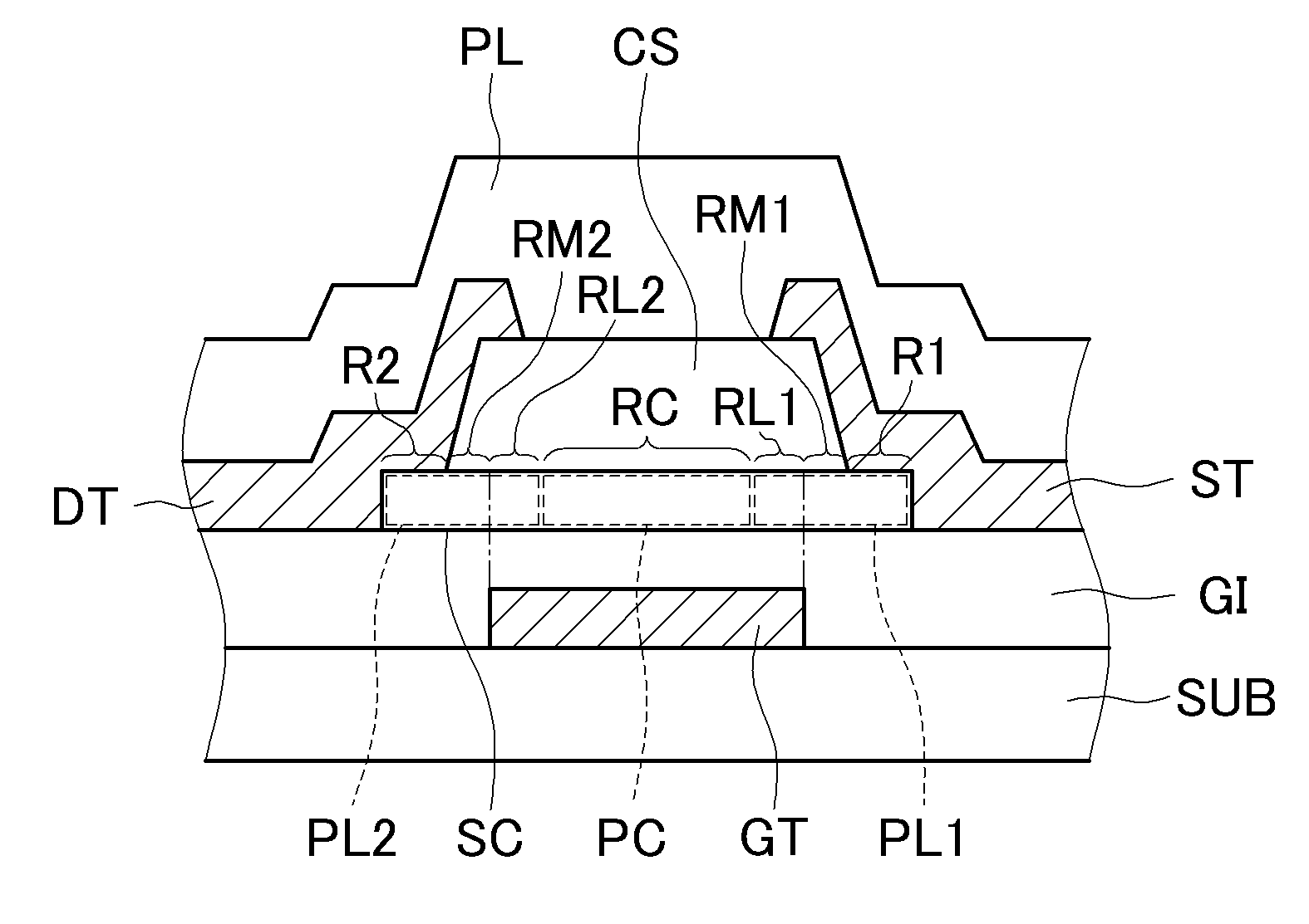
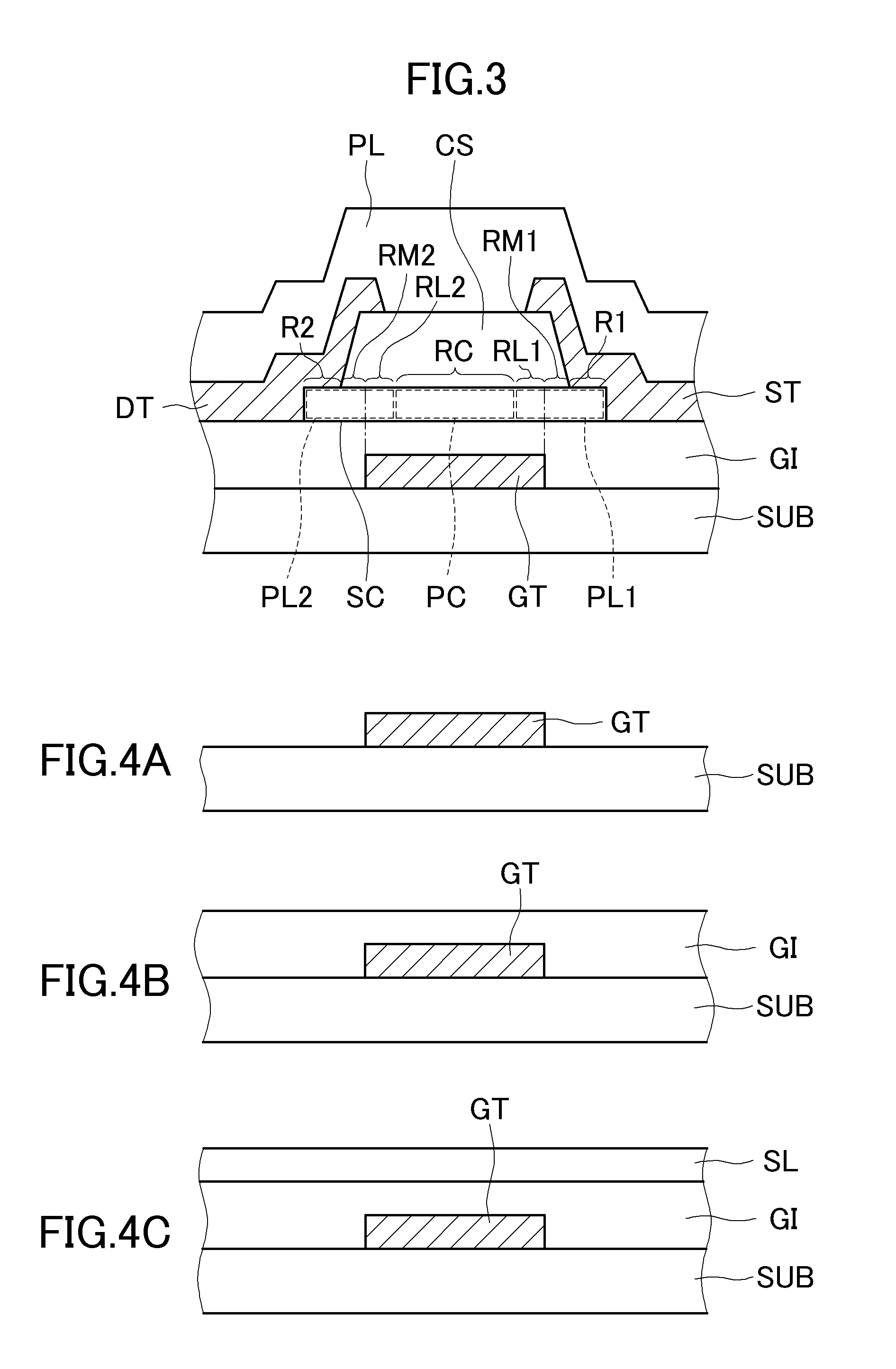
[0025]Hereinafter, an embodiment of the present invention is described with reference to the drawings. Of the components described herein, components having the same function are denoted by the same reference character, and description thereof is omitted. Note that, the embodiment to be described hereinafter is an example of a case where the present invention is applied to an in-plane-switching (IPS) type liquid crystal display device.

[0026]A display device according to this embodiment is a liquid crystal display device including an array substrate, a filter substrate, which is opposed to the array substrate and includes a color filter, a liquid crystal material sealed in a space sandwiched between both the substrates, and a driver IC mounted on the array substrate. The array substrate and the filter substrate are each an insulating substrate such as a glass substrate, which has been subjected to processing.

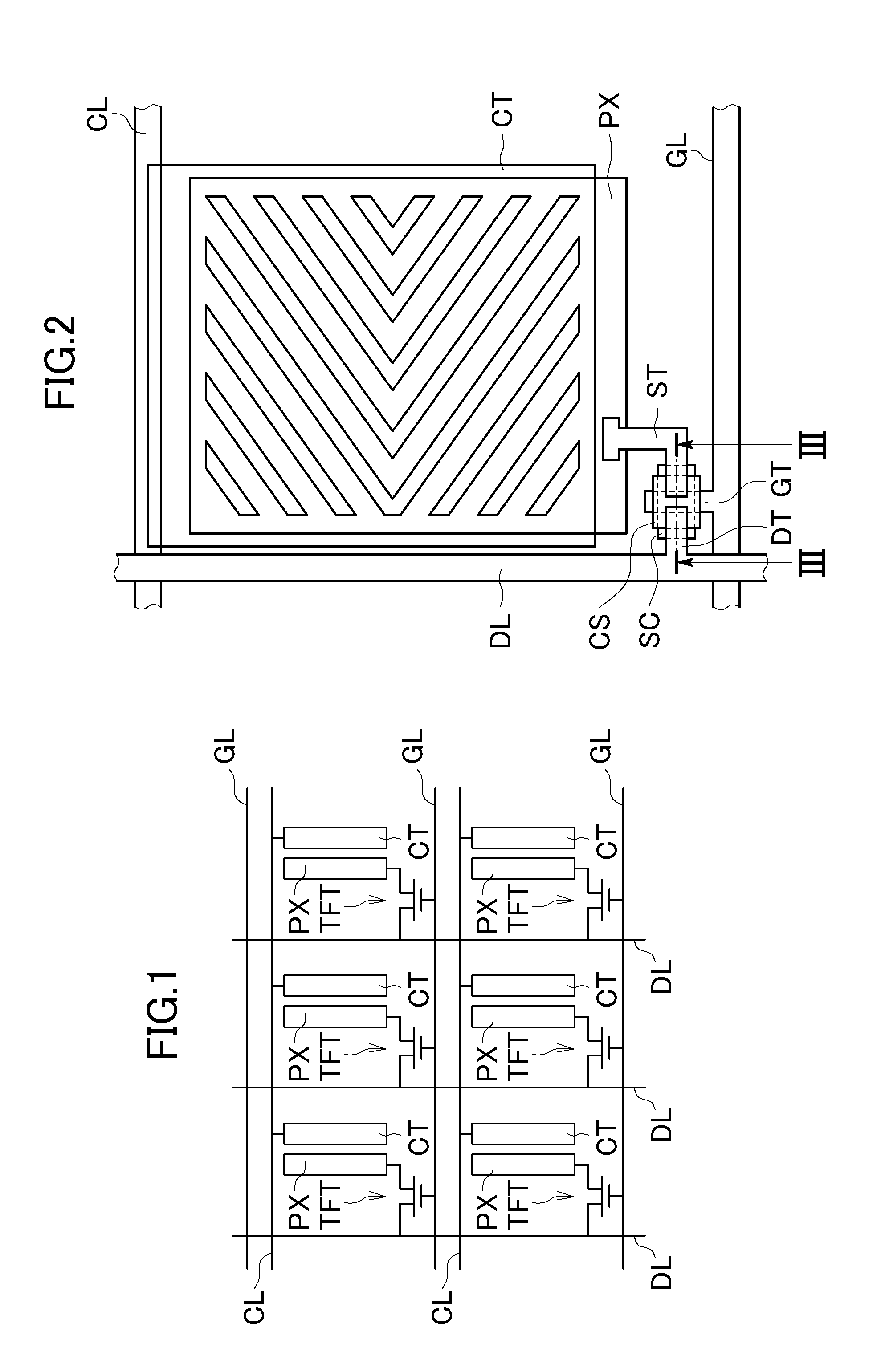
[0027]FIG. 1 is a circuit diagram illustrating an equivalent circuit of the ...


PUM


Abstract

Provided a display device including a thin film transistor. The thin film transistor includes a gate electrode, a gate insulating layer which covers the gate electrode, an oxide semiconductor film above the gate insulating layer, a source electrode and a drain electrode which are respectively provided in contact with a first region and a second region, which are provided in the upper surface of the oxide semiconductor film, and a channel protective film which is provided in contact with a third region between the first region and the second region. In plan view, a region of the oxide semiconductor film, which overlaps with the gate electrode, is smaller than the third region, and a portion of the oxide semiconductor film except for a portion which overlaps with the gate electrode has a resistance lower than the portion.

Description

CROSS-REFERENCE TO RELATED APPLICATION[0001]The present application claims priority from Japanese application JP 2011-190006 filed on Aug. 31, 2011, the content of which is hereby incorporated by reference into this application.BACKGROUND OF THE INVENTION[0002]1. Field of the Invention[0003]The present invention relates to a display device and a manufacturing process of a display device.[0004]2. Description of the Related Art[0005]In recent years, a display device utilizing a thin film transistor using an oxide semiconductor has been actively developed. The display device includes pixel circuits arranged in matrix. This development is made for improving characteristics of the display device. Japanese Patent Application Laid-open No. 2009-272427 discloses a thin film transistor having a channel etch stop structure which uses the oxide semiconductor.SUMMARY OF THE INVENTION[0006]The oxide semiconductor is liable to change its characteristics by a material that is provided in contact w...

Claims


Application Information

Patent Timeline
IPC IPC(8): H01L33/36H01L21/34
CPCH01L29/7869H01L27/1225G02F1/1368H01L29/786H01L29/78618H01L29/78696H01L27/12H01L29/78606H01L29/66742
Inventor NODA, TAKESHIKAWAMURA, TETSUFUMI
Owner JAPAN DISPLAY INC
Why Eureka
Try Eureka