Semiconductor device and manufacturing method thereof

a technology of semiconductors and semiconductors, applied in the direction of semiconductor devices, electrical devices, transistors, etc., can solve the problems of reducing the ntbi performance of the device, limiting the threshold voltage vt of the device, and reducing the device performance, so as to prolong the ntbi life of the device, improve the reliability of the device, and improve the ntbi performance.

Inactive Publication Date: 2013-02-28
SEMICONDUCTOR MANUFACTURING INTERNATIONAL (BEIJING) CORP
View PDF4 Cites 8 Cited by
  • Summary
  • Abstract
  • Description
  • Claims
  • Application Information

AI Technical Summary

Benefits of technology

[0030]According to an embodiment of the present invention, there is provided a novel method of manufacturing a semiconductor device. According to one embodiment of the present invention, device reliability, especially the NTBI performance, can be improved; which in turn can prolong the NBTI life of the device. According to another embodiment of the present invention, the introduced P-type impurities can offset or cancel the influence on the gate material layer exerted by the N-type dopant introduced and can also be used to fine-tune the depletion region of the PMOS gate material layer. As such, a larger dosage of fluorine can be introduced into the Si / SiO2 interface, thereby improving NBTI performance of the device. According to a further embodiment of the present invention, the influence on the subsequent manufacturing process steps of the device, exerted by the introduction of fluorine can be mitigated or eliminated such that the solution of the present invention can be combined with the existing process cycles without substantively changing the process parameters of the subsequent process cycles.

Problems solved by technology

However, the threshold voltage Vt of a device is limited, and cannot be unlimitedly decreased.
The scaling down of gate dielectric thickness with a high rate and scaling down of threshold voltage with a lower rate has resulted in degradation of the device performance such as the Negative Bias Temperature Instability (NBTI) so that the device fails to meet the specification.
However, pure fluorine implantation may cause bubble defects when the dosage is too high.
In other words, the fluorine dosage is limited if pure fluorine implantation is employed, and thus, the improvement of the NBTI performance by such fluorine implantation is limited.

Method used


Image

  • Semiconductor device and manufacturing method thereof
  • Semiconductor device and manufacturing method thereof
  • Semiconductor device and manufacturing method thereof

Examples


Embodiment Construction

[0036]The embodiments of the present invention are described in conjunction with the figures.

[0037]Hereinafter, a method of manufacturing a semiconductor device according to the embodiments of the present invention are described with reference to FIGS. 1-3.

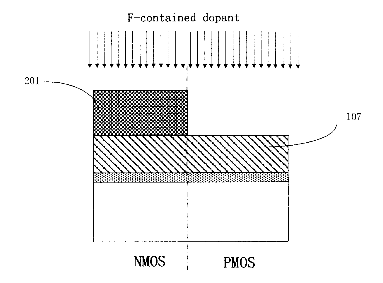
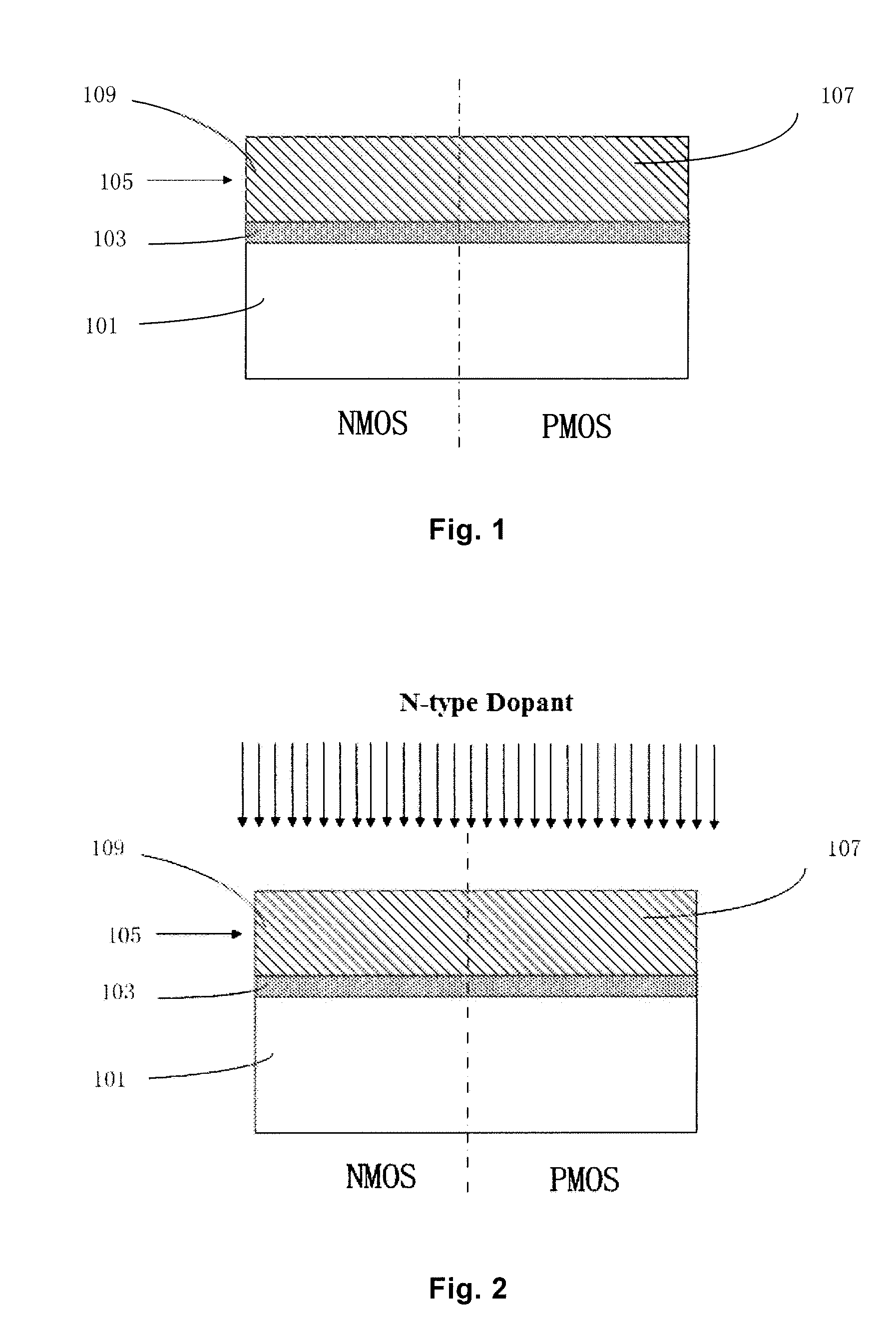
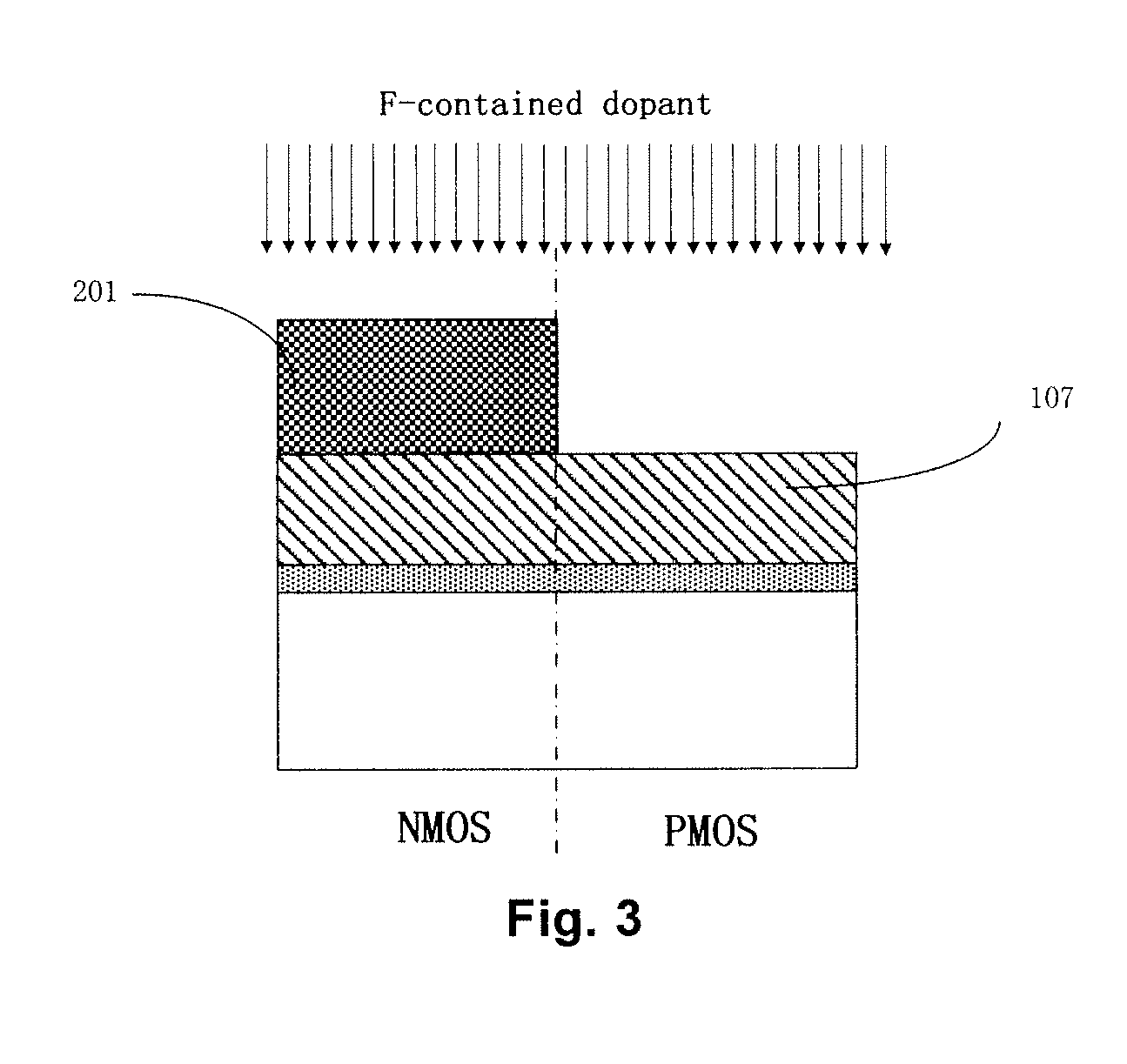
[0038]The semiconductor device can comprise a PMOS device. In addition to the PMOS device, the semiconductor device can further comprise an NMOS device (as shown in FIG. 1) and / or any other active or passive device (not shown).

[0039]As shown in FIGS. 1-3, the reference “PMOS” corresponds to a PMOS device, while the reference “NMOS” corresponds to an NMOS device. In addition, although the NMOS device is shown as abutting the PMOS device in some of the figures, it is merely illustrative and not limiting. The NMOS device or other devices also can be separate from the PMOS device.

[0040]Further, for the sake of clarity, N-well or P-well field oxide isolation or trench isolation (e.g. STI) are not shown in the figures, because these are...


PUM


Abstract

The present invention relates to a semiconductor device having a P-channel semiconductor region and a manufacturing method therefor. The method comprises: forming a gate dielectric layer on a substrate; forming a gate material layer on the gate dielectric layer; blanket pre-doping the gate material layer to introduce an N-type dopant thereto; and pre-doping with fluorine a region of the gate material layer designed to be said P-channel semiconductor device, such that the fluorine dopes an interface between the substrate and the region of the gate dielectric layer designated to be said P-channel semiconductor device. The semiconductor device further comprises an N-type semiconductor region in said gate material layer.

Description

CROSS-REFERENCE TO RELATED APPLICATIONS[0001]This application claims priority to Chinese Patent Application No. 201110248458.5, filed on Aug. 26, 2011 and entitled “Semiconductor Device and Manufacturing Method thereof”, which is incorporated herein in its entirety by reference.FIELD OF THE INVENTION[0002]The present invention relates to the field of semiconductor fabrication techniques, and more specifically, relates to a semiconductor device and a manufacturing method thereof.DESCRIPTION OF THE RELATED ART[0003]With the continuous reduction in size of ultra-large scale integrated circuits (ULSI), gate dielectrics in a MOS (metal-oxide-semiconductor) device are being scaled down in thickness to achieve higher device performance. However, the threshold voltage Vt of a device is limited, and cannot be unlimitedly decreased. Currently, the gate voltage Vg is about 1.0V, which has reached a plateau.[0004]The scaling down of gate dielectric thickness with a high rate and scaling down of...

Claims


Application Information

Patent Timeline
Patent Type & Authority Applications(United States)
IPC IPC(8): H01L27/092H01L21/28
CPCH01L21/26506H01L21/28035H01L29/66545H01L29/4916H01L29/51H01L21/28176
Inventor FENG, JUNHONGGAN, ZHENGHAO
Owner SEMICONDUCTOR MANUFACTURING INTERNATIONAL (BEIJING) CORP
Why Eureka
Try Eureka