Switching power supply device and semiconductor device

a technology of switching power supply and semiconductor, which is applied in the direction of electric variable regulation, process and machine control, instruments, etc., can solve the problems of large power loss, typical energy loss of switching power supply under light load, power loss in switching elements b>2, etc., and achieve the effect of reducing the loss of intermittent resumption

Active Publication Date: 2013-02-28
PANASONIC SEMICON SOLUTIONS CO LTD
View PDF7 Cites 38 Cited by
  • Summary
  • Abstract
  • Description
  • Claims
  • Application Information

AI Technical Summary

Benefits of technology

[0059]When a switching element intermittently carries out a switching operation to supply and cut an input DC voltage to convert the input DC voltage to a regulated output DC voltage, the semiconductor device of the present invention (i) times a bottom-monitoring time period as soon as an instruction is given to execute the switching operation in the intermittent resumption for resuming the switching operation, and (ii) turns ON the switching element at a bottom of the ringing voltage detected while the bottom-monitoring time period is being timed.
[0060]This feature successfully reduces the risk of a conventional problem that the switching element turns ON at a high voltage and not at a bottom of the ringing voltage when the switching element turns ON as soon as an instruction is given to execute the switching operation after the elapse of a waiting time period to be timed as soon as an instruction is given to suspend the switching operation no matter whether or not the bottom of the ringing voltage is detected. As a result, the feature successfully reduces a loss in the intermittent resumption by the capacitance between the input and the output of the switching element.

Problems solved by technology

In most cases, a typical energy loss of a switching power supply under the light load, such as a stand-by load, is due to a switching loss caused by a switching operation.
The above conventional technique, however, causes the following problem: When the signal Enable goes high, the intermittent resuming circuit 91 outputs the signal Up in order to resume the switching operation in the intermittent oscillation control, regardless of the ringing voltage developed in the switching element 2.
This problem leads to a power loss in the switching element 2.
However, in the case where a voltage is high when the switching element 2 turns ON in the intermittent resumption, the capacitance C inevitably causes a large power loss as a result.
In particular, when the intermittent control cycle is made shorter depending on the state of a load, the power loss becomes greater.

Method used


Image

  • Switching power supply device and semiconductor device
  • Switching power supply device and semiconductor device
  • Switching power supply device and semiconductor device

Examples


embodiment 1

[0082]Described here is a switching power supply device according to Embodiment 1 of the present invention.

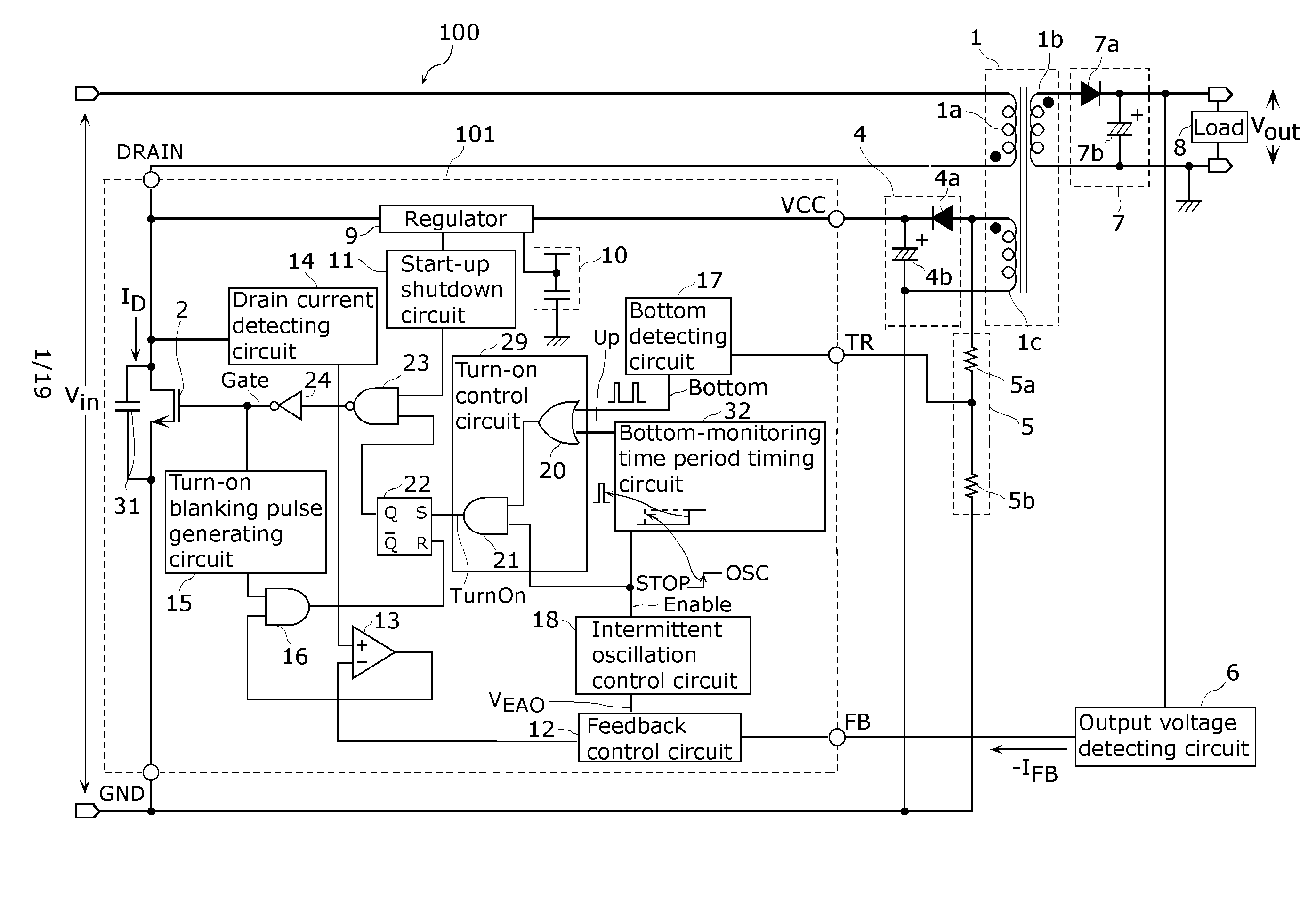
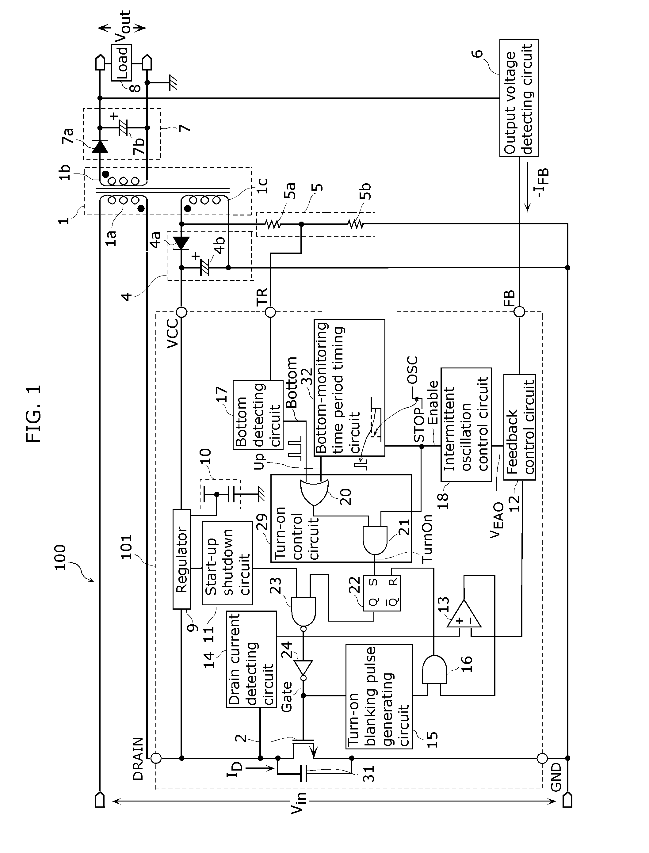
[0083]FIG. 1 depicts a circuit diagram exemplifying a structure of a switching power supply device 100 including a semiconductor device 101 according to Embodiment 1 of the present invention. The semiconductor device 101 works as a control circuit for the switching power supply device 100. Hereinafter, the control circuit implemented by the semiconductor device 101 is referred to as a control circuit 101 having the same numerical sign as the semiconductor device has

[0084]In FIG. 1, a transformer 1 has a primary winding 1a, a secondary winding 1b, and an auxiliary winding 1c. Polarities between the primary winding 1a and the secondary winding 1b are reversed. An alternating current (AC) voltage obtained from the secondary winding 1b is converted into an output direct current (DC) voltage by an output voltage generating unit 7 including a rectifying diode 7a and a capacitor 7b. T...

embodiment 2

[0174]Described next is a switching power supply device according to Embodiment 2 of the present invention.

[0175]FIG. 8 depicts a circuit diagram exemplifying a structure of a switching power supply device 200 including a semiconductor device 201 according to Embodiment 2 of the present invention. The semiconductor device 201 works as a control circuit for the switching power supply device 200. Hereinafter, the control circuit implemented by the semiconductor device 201 is referred to as a control circuit 201 having the same numerical sign as the semiconductor device has.

[0176]A comparison between the control circuit 201 according to Embodiment 2 and the control circuit 101 according to Embodiment 1 shows that the control circuit 201 has a bottom-monitoring time period timing circuit 33 additionally including a ringing cycle measuring circuit 34.

[0177]In Embodiment 1, the bottom-monitoring time period timing circuit 32 measures the bottom-monitoring time period t expressed in Expres...

embodiment 3

[0202]Described here is a switching power supply device according to Embodiment 3 of the present invention.

[0203]FIG. 11 depicts a circuit diagram exemplifying a structure of a switching power supply device 300 including a semiconductor device according to Embodiment 3 of the present invention. A semiconductor device 301 works as a control circuit for the switching power supply device 300. Hereinafter, the control circuit implemented by the semiconductor device 301 is referred to as a control circuit 301 having the same numerical sign as the semiconductor device has.

[0204]Compared with the control circuit 101 according to Embodiment 1, the control circuit 301 according to Embodiment 3 additionally has an oscillating circuit 26, and includes a bottom-monitoring time period timing circuit 35 instead of the bottom-monitoring time period timing circuit 32.

[0205]It is noted that the switching power supply device 100 according to Embodiment 1 and the switching power supply device 200 acco...


PUM


Abstract

In a switching power supply device which intermittently executes a switching operation, a power loss which occurs in resumption of the switching operation is reduced. A semiconductor device works as a control circuit for the switching power supply device, and includes: an intermittent oscillation control circuit which alternately gives an instruction for execution and suspension of the switching operation of a switching element; a bottom detecting circuit which detects a bottom of a ringing voltage that develops when the switching element is OFF; a bottom-monitoring time period timing circuit which times a bottom-monitoring time period starting as soon as the instruction for the execution of the switching operation is given; and a turn-on control circuit which turns ON, before the timing of the bottom-monitoring time period ends, the switching element only when the bottom of the ringing voltage is detected.

Description

TECHNICAL FIELD[0001]The present invention relates to (i) a switching power supply device which generates a regulated output voltage by causing a switching element to intermittently execute a switching operation to supply and cut an input voltage and (ii) a semiconductor device for controlling the switching power supply device.BACKGROUND ART[0002]Switching power supply devices including semiconductor devices have been widely used for household equipment, such as electric appliances, as its power supply devices in order to reduce its electric consumption and improve its power efficiency. The semiconductor devices utilize a switching operation performed by semiconductor (a switching element, such as a transistor) to control (to stabilize) an output voltage.[0003]Recently, in particular, global warming prevention measures have drawn a significant attention to the reduction of the stand-by electricity consumed by electric devices, such as the household appliances. This trend generates a...

Claims


Application Information

Patent Timeline
Patent Type & Authority Applications(United States)
IPC IPC(8): H02M3/335
CPCH02M1/36Y02B70/1491H02M2001/0048H02M3/33523H02M1/0048Y02B70/10
Inventor YAMASHITA, TETSUJI
Owner PANASONIC SEMICON SOLUTIONS CO LTD
Why Eureka
Try Eureka