Organic Light-Emitting Display Device and Method of Fabricating the Same

a light-emitting display and organic technology, applied in the direction of semiconductor/solid-state device manufacturing, semiconductor devices, electrical apparatus, etc., can solve the problem of non-uniform brightness across the entire device, image produced by the device, etc., to achieve the effect of enhancing brightness uniformity and reducing the resistance of cathode electrodes

Inactive Publication Date: 2013-03-07
LG DISPLAY CO LTD
View PDF5 Cites 99 Cited by
  • Summary
  • Abstract
  • Description
  • Claims
  • Application Information

AI Technical Summary

Benefits of technology

[0016]An organic electro-luminescence device capable of reducing a resistance of a cathode electrode to enhance brightness uniformity at each location within the device is described. The organic electro-luminescence device includes a bank layer formed over a substrate, the bank layer including a first, second, and third portion. A first electrode is formed between the first and second portions of the bank layer. An auxiliary electrode is formed where at least a part of the auxiliary electrode is formed between the second and third portions of the bank layer. A pattern is formed on the auxiliary electrode. An organic material layer is formed between the first and second portions of the bank layer. A second electrode is formed on the organic material layer, where at least a portion of the second electrode is electrically coupled to the auxiliary electrode.

Problems solved by technology

As a result, a brightness difference may be created between an edge region of the panel and a central portion thereof This causes the image produced by the device to appear nonuniform with respect to brightness across the entire device.

Method used


Image

  • Organic Light-Emitting Display Device and Method of Fabricating the Same
  • Organic Light-Emitting Display Device and Method of Fabricating the Same
  • Organic Light-Emitting Display Device and Method of Fabricating the Same

Examples


Embodiment Construction

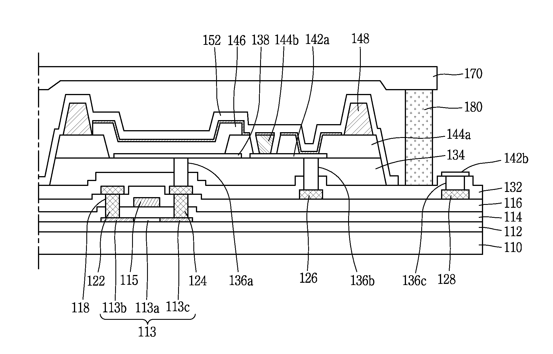
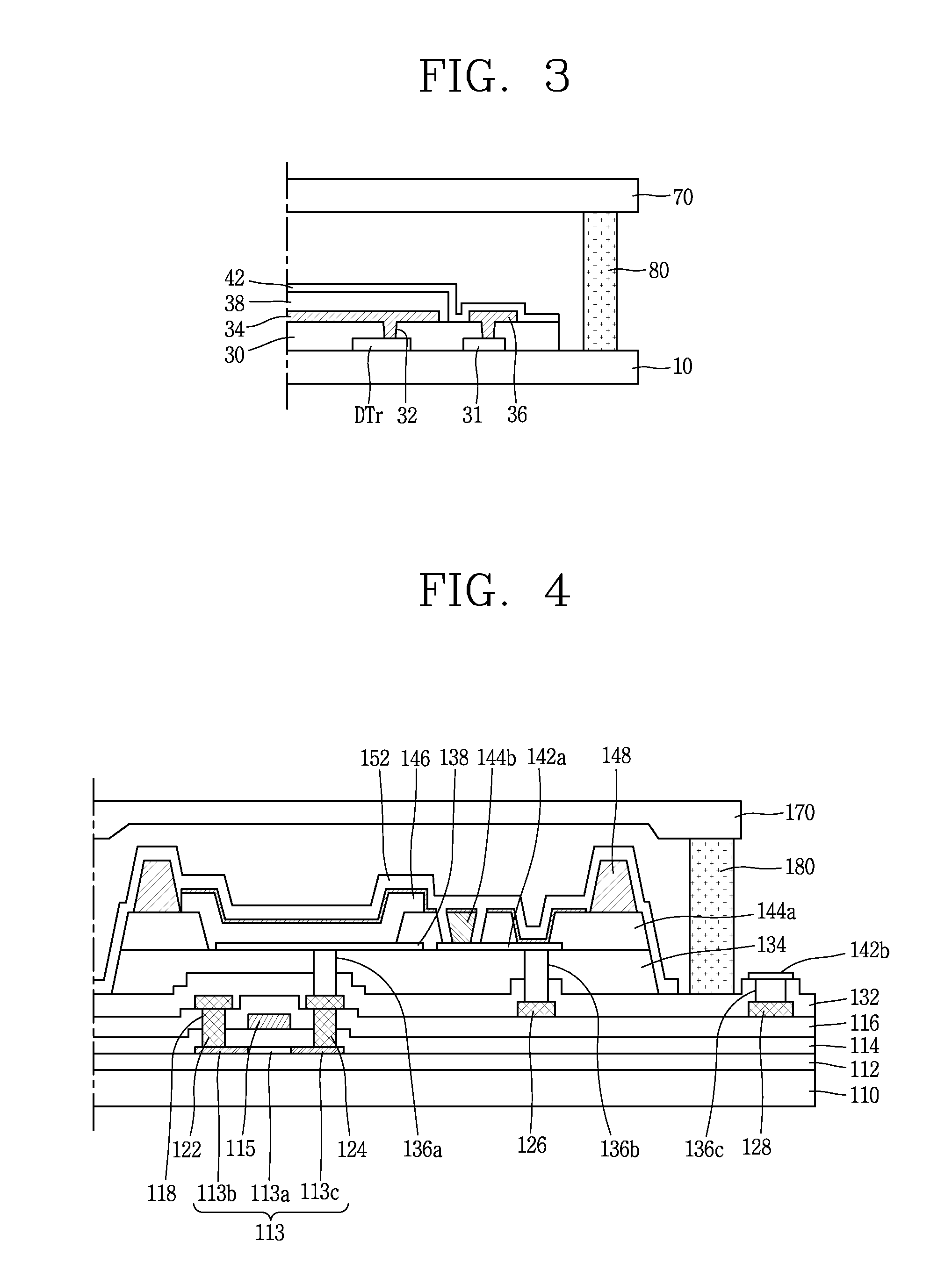
[0025]FIG. 4 is a cross-sectional view illustrating one pixel area including a driving thin-film transistor of an organic electro-luminescence device according to an embodiment of the present invention. FIG. 5 is a cross-sectional view illustrating an actual voltage drop prevention pattern and bank. FIGS. 6A through 6E are plan views illustrating the shape of a voltage drop prevention pattern according to embodiments of the present invention.

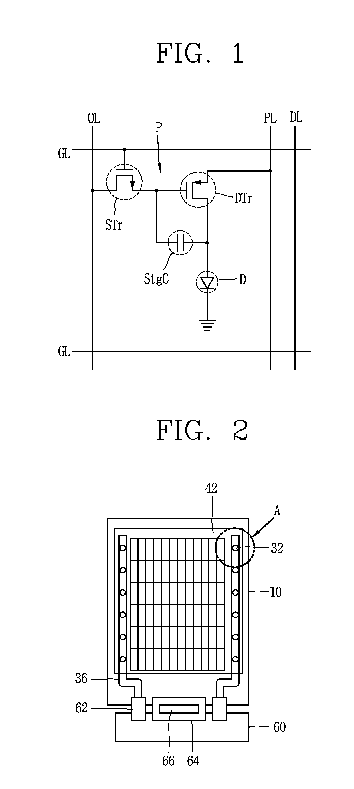
[0026]Referring to FIG. 4, an organic electro-luminescence device according to an embodiment of the present invention is a top emission type, and includes driving and switching transistors (DTr) (as described below, 113, 114, and 115 in combination form the transistors), a first substrate 110 formed with an organic electro-luminescence diode (D), and a second substrate 170 for encapsulation.

[0027]A buffer layer 112 is formed on a driving area (DA) of the first substrate 110. A semiconductor layer 113 consisting of a first area 113a with pure pol...


PUM


Abstract

An organic electro-luminescence device capable of reducing a resistance of a cathode electrode to enhance brightness uniformity at each location within the device is described. The organic electro-luminescence device includes a bank layer formed over a substrate, the bank layer including a first, second, and third portion. A first electrode is formed between the first and second portions of the bank layer. An auxiliary electrode is formed where at least a part of the auxiliary electrode is formed between the second and third portions of the bank layer. A pattern is formed on the auxiliary electrode. An organic material layer formed between the first and second portions of the bank layer. A second electrode formed on the organic material layer, where at least a portion of the second electrode is electrically coupled to the auxiliary electrode.

Description

CROSS REFERENCE TO RELATED APPLICATION[0001]This application claims the benefit of Korean Patent Application No. 10-2011-0089277, filed on Sep. 2, 2011, which is hereby incorporated by reference in its entirety.BACKGROUND OF THE DISCLOSURE[0002]1. Field of the Disclosure[0003]The present invention relates to an organic electro-luminescence device and a method of fabricating the same.[0004]2. Discussion of the Related Art[0005]In recent years, there has been increased use of portable electronic devices such as notebooks and personal mobile devices. These devices include display devices. In order to maximize their per-battery charge lifespan, ideally these display device are constructed using light weight and low power consumption technologies, for example using flat panel displays (FPDs) such as liquid crystal displays (LCD) and organic electro-luminescence devices.[0006]Organic electro-luminescence devices have advantages over other display technologies including, for example, havin...

Claims


Application Information

Patent Timeline
Patent Type & Authority Applications(United States)
IPC IPC(8): H01L33/62
CPCH01L27/3246H01L51/5212H10K59/1315H10K59/122H10K50/814H10K50/824H01L21/02107H10K50/805
Inventor LEE, JOON-SUKKIM, SE-JUNE
Owner LG DISPLAY CO LTD
Why Eureka
Try Eureka