Method of Producing Template for Epitaxial Growth and Nitride Semiconductor Device

a semiconductor device and epitaxial growth technology, applied in the direction of crystal growth process, polycrystalline material growth, semiconductor laser, etc., can solve the problems of increasing manufacturing costs, reducing output, and difficult processing of sapphire substrates, so as to reduce threading dislocation density , the effect of easy optimization

Active Publication Date: 2013-03-21
NIKKISO COMPANY
View PDF5 Cites 12 Cited by
  • Summary
  • Abstract
  • Description
  • Claims
  • Application Information

AI Technical Summary

Benefits of technology

[0041]According to the method for producing a template for epitaxial growth or the nitride semiconductor device having the above-described characteristics, provided is an AlGaN layer having a fine and flat surface and a reduced threading dislocation density, that is epitaxially grown on a sapphire (0001) substrate having recesses and protrusions on its surface by an epitaxial lateral overgrowth method at a temperature below 1,300° C., lower than conventional growth temperatures. Specifically, the initial-stage AlN layer, as an underlying layer for the first ELO layer (AlN layer) and the second ELO layer (AlGaN layer) that are sequentially epitaxially grown thereon by an epitaxial lateral overgrowth method, has portions that are epitaxially grown from the flat surfaces of the protrusion tops, and are C+-axis oriented. Specifically, the surface of the initial-stage AlN layer is an Al polar face uniformly. Thus, even at a growth temperature below 1,300° C., a layer having a fine and flat surface and a reduced threading dislocation density can be obtained as the first ELO layer and the second ELO layer that are epitaxially grown thereon by an epitaxial lateral overgrowth method.
[0042]Particularly, the lateral overgrowth of the first ELO layer is stopped before the recess upper region is completely covered. The first ELO layer including an AlN layer, with its growth condition being easily optimized, is previously laterally grown and then the second ELO layer starts to laterally grow right before the recess upper region is completely covered by the lateral overgrowth, so that the lateral overgrowth condition of the second ELO layer can be optimized more than in the case where only the second ELO layer is laterally and directly grown on the initial-stage AlN layer. In the lateral overgrowth of the first ELO layer and the second ELO layer, a region (lower layer region of the recess upper region) that is covered from both sides with the first ELO layer, laterally grown from two adjacent protrusion tops sandwiching a new recess of the initial-stage AlN layer is, firstly, formed in a mesa-shape (the cross sectional shape perpendicular to the stretching direction of the recess is trapezoidal) above the new recess. The mesa-shaped upper surface opening gradually narrows as the lateral overgrowth of the first ELO layer progresses. However, the lateral overgrowth of the first ELO layer is stopped before the opening is completely closed with the first ELO layer; then, the lateral overgrowth of the second ELO layer is started; and finally, the second ELO layer laterally grown from the upper surface of the first ELO layer on both sides sandwiching the opening, coalesces over the opening, thereby closing the opening. Closing points of the openings (coalescing points of the second ELO layer) stretch in a ridgeline along the stretching direction of the recesses. Normally, wedge-shaped voids having the ridgeline at the tops are formed at the top portion of the recess upper region. It is conceivable that compressive strain is generated in a lateral direction from both sides near the closing points of the openings and at the upper portions thereof. The properties of the crystal surface under the condition where the compressive strain is generated, heavily depend on surface energy, strains, crystal growth conditions, etc. Therefore, in order to obtain preferable surface properties, growth conditions need to correspond to compressive strains, but it is realized that, by starting the lateral overgrowth of the second ELO layer right before the recess upper region is completely covered, the lateral overgrowth condition of the second ELO layer can be easily optimized. Moreover, since the growth of the first ELO layer can be stopped before the recess upper region is completely covered, the growth condition of the first ELO layer can be set without considering the condition of completely covering the recess upper region, so that an optimized range of the lateral overgrowth condition is wider than in the case where only the first ELO layer is directly and laterally grown from the upper surface of the initial-stage AlN layer and then completely covers over new recesses.
[0043]As a result, an AlGaN nitride semiconductor layer of high crystal quality is stably provided as a top layer of the template for the epitaxial growth having the above-described characteristics without increasing manufacturing costs, and thus a semiconductor device having the AlGaN nitride semiconductor layer will have superior performances.

Problems solved by technology

Thus, the AlN underlying layer and the ELO-AlN layer cannot be grown continuously, and the manufacturing process becomes complex and the throughput decreases, thereby increasing manufacturing costs.
However, the sapphire substrate has a low etching rate and is difficult to process, so that an ELO-AlN layer having a low threading dislocation density needs to be grown on a shallow-grooved substrate.

Method used


Image

  • Method of Producing Template for Epitaxial Growth and Nitride Semiconductor Device
  • Method of Producing Template for Epitaxial Growth and Nitride Semiconductor Device
  • Method of Producing Template for Epitaxial Growth and Nitride Semiconductor Device

Examples


examples 2 to 4

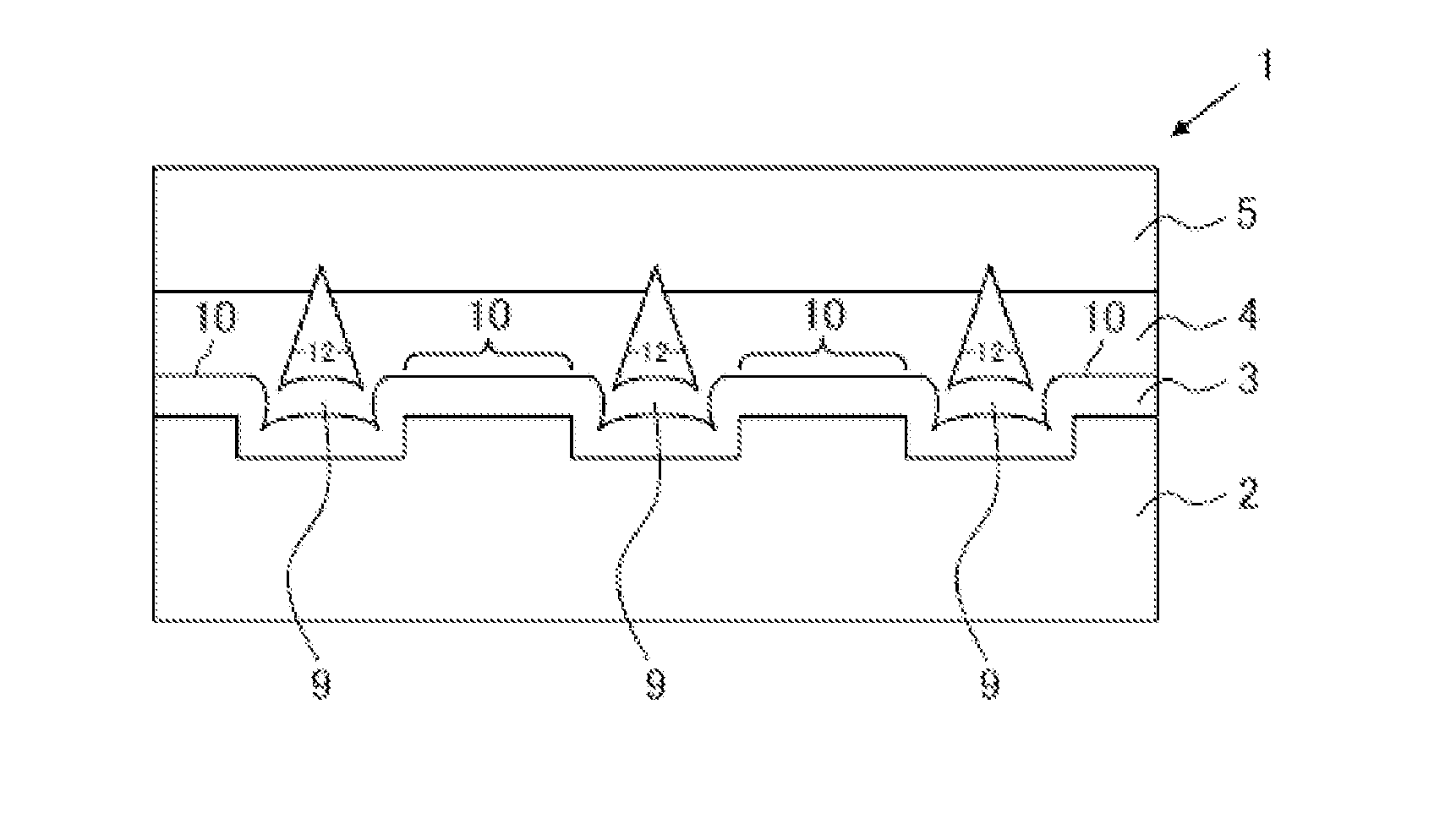
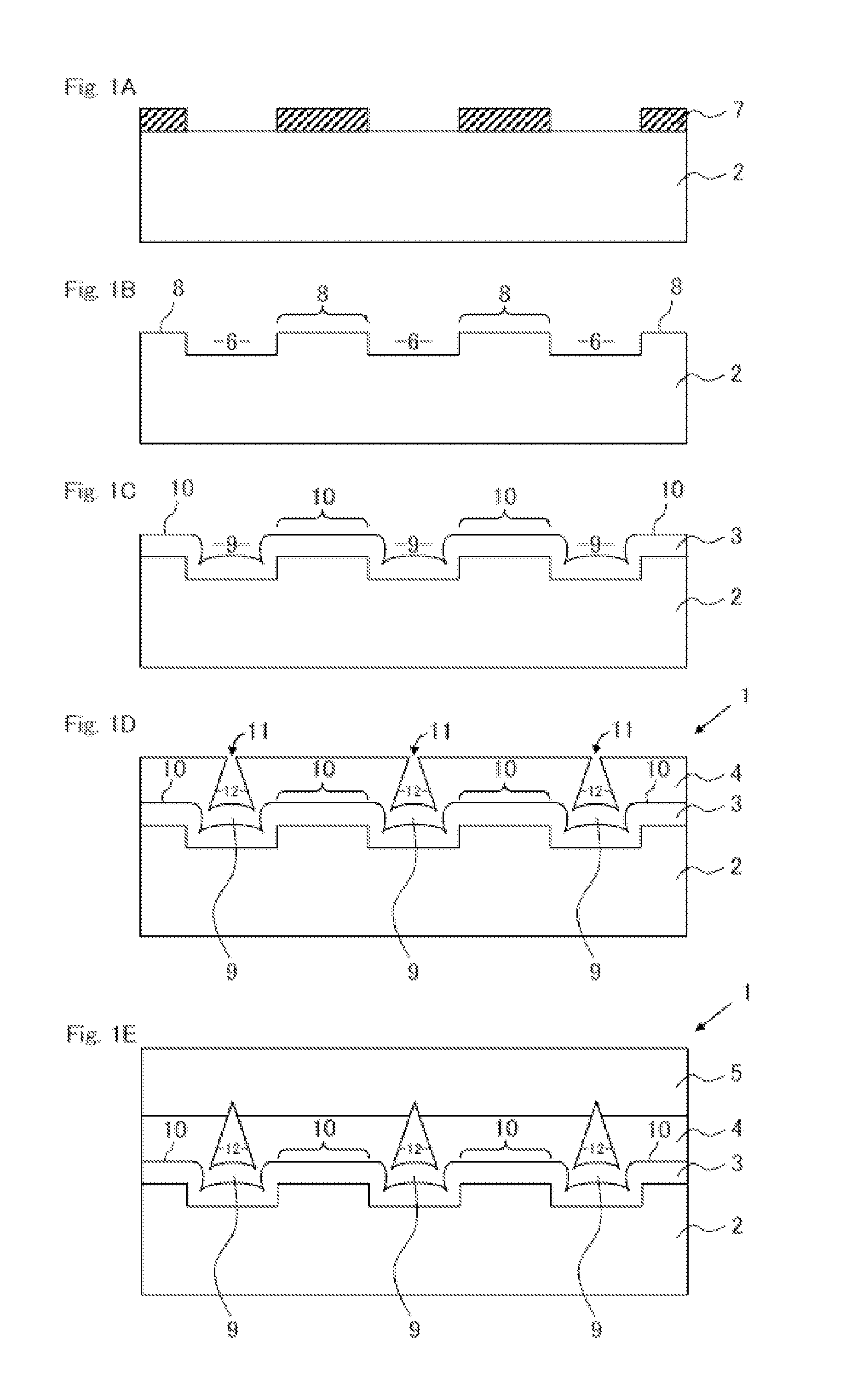
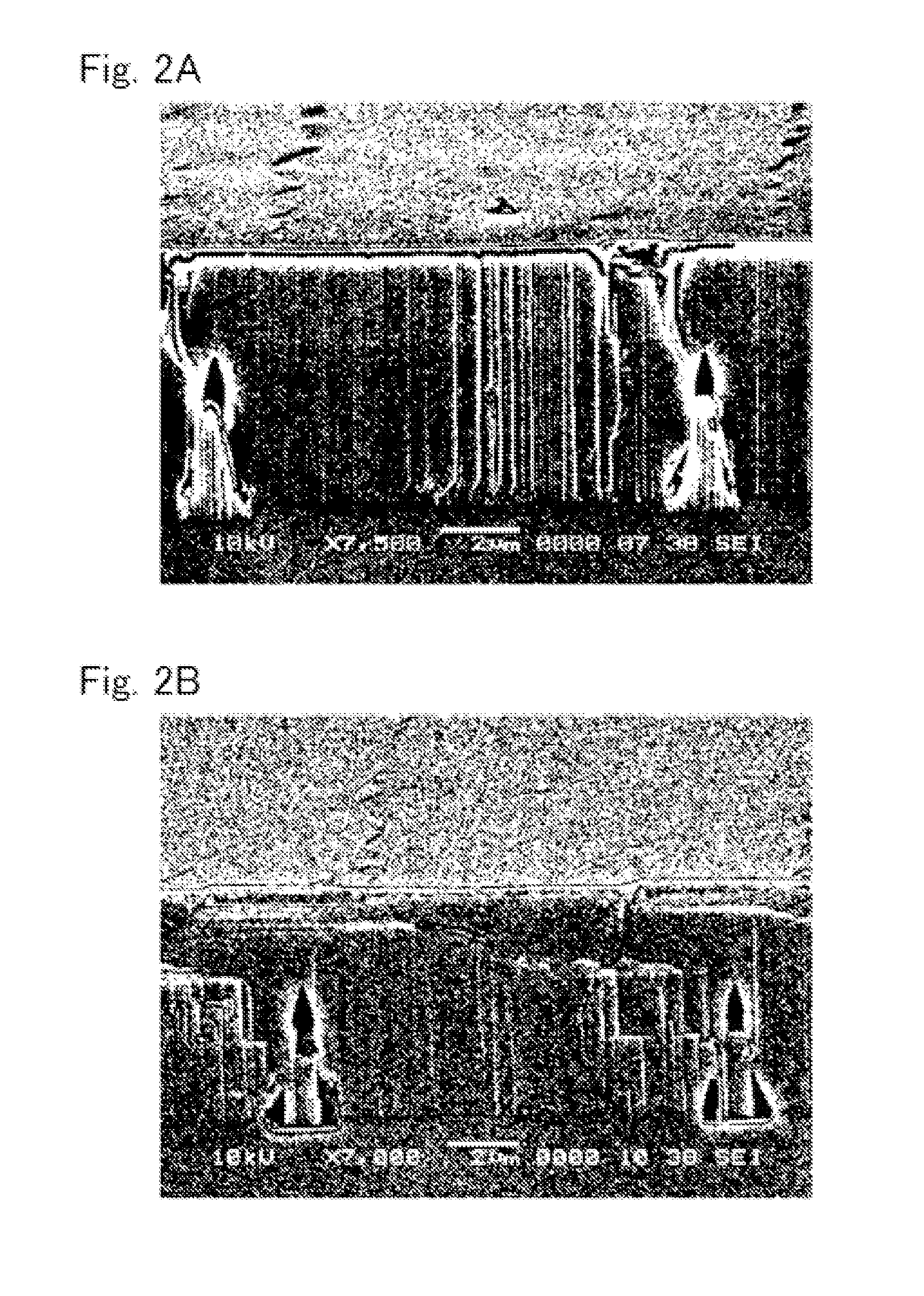
[0077]FIGS. 6A and 6B, FIGS. 7A and 7B, and FIGS. 8A and 8B show the SEM images (cross-sectional views (A) and bird's-eye views (B)) of Examples 2 to 4 in sequence. In Example 2, the width, interval, and depth of the grooves 6 formed on the surface of the sapphire substrate 2 are 2 μm, 5 μm, and 0.3 μm, respectively; in Example 3, the width, interval, and depth are 2 μm, 10 μm, and 0.3 μm, respectively; and in Example 4, the width, interval, and, depth are 3 μm, 5 μm, and 0.3 μm, respectively, so that the sapphire substrates 2 have different recessed-and-protruded structures thereon. In Examples 2 to 4, the growth conditions (growth temperature and flow ratio) of the initial-stage AlN layer 3, the first ELO layer 4, and the second ELO layer 5 are set to be the same, respectively. The thicknesses of the initial-stage AlN layer 3, the first ELO layer 4, and the second ELO layer 5 are 1.5 μm, 1.8 μm, and 1.8 μm, respectively, in Example 2; the thicknesses are 1.5 μm, 1.8 μm, and 2.3 μm...

example 5 and example 6

[0083]FIG. 11 shows the SEM image (bird's-eye view) of Example 5. FIG. 12 shows the differential interference microscopic image showing the state where the recess upper region is not completely covered after the first ELO layer 4 of Example 6 is formed. In Example 5 and Example 6, the width, interval, and depth of the grooves 6 formed on the surface of the sapphire substrate 2 are 2 μm, 10 μm, and 0.3 μm, respectively. The growth conditions (growth temperature and flow ratio) of the initial-stage AlN layer 3, the first ELO layer 4, and the second ELO layer 5 are set to be the same, respectively. The thicknesses of the initial-stage AlN layer 3, the first ELO layer 4, and the second ELO layer 5 are 1.6 μm, 2.1 μm, and 4.5 μm, respectively, in Example 5, and are 1.3 μm, 1.8 μm, and 1.5 μm, respectively, in Example 6. The void height of Example 5 is 3.7 μm. The Al molar fractions x of the second ELO layer 5 in Example 5 and Example 6 are 0.9, respectively.

[0084]Example 5 is different f...


PUM


Abstract

A surface of a sapphire (0001) substrate is processed so as to have recesses and protrusions so that protrusion tops are made flat and have a given plan-view pattern. An initial-stage AlN layer is epitaxially grown on the surface of the sapphire (0001) substrate so that new recesses are formed over the recesses, by performing C axis orientation control so that a C+ axis oriented AlN layer grows on flat surfaces of the protrusion tops, excluding edges. A first ELO layer including an AlN (0001) layer is epitaxially grown on the initial-stage AlN layer by an epitaxial lateral overgrowth method, and stops growing before a recess upper region above the new recesses is completely covered with the first ELO layer that is laterally grown from a protrusion upper surface of the initial-stage AlN layer. A second ELO layer including an AlxGa1-xN (0001) layer (1>x>0) is epitaxially grown on the first ELO layer by an epitaxial lateral overgrowth method. The recess upper region is completely covered with the second ELO layer that is laterally grown from an upper surface of the first ELO layer.

Description

CROSS-REFERENCE TO RELATED APPLICATIONS[0001]This application is a National Phase filing under 35 U.S.C. §371 of International Application No. PCT / JP2010 / 059589 filed on Jun. 7, 2010.TECHNICAL FIELD[0002]The present invention relates to a method for producing a template for epitaxial growth as an underlying substrate where a GaN compound semiconductor layer (general formula: AlxGayIn1-x-yN) is epitaxially grown, and also relates to a nitride semiconductor device.BACKGROUND ART[0003]GaN nitride semiconductor devices such as light-emitting diodes and semiconductor lasers are conventionally produced by growing a multi-layered GaN compound semiconductor layer on a template for epitaxial growth (for example, see Non-patent Document 1). FIG. 15 illustrates a typical crystal layer structure of a conventional GaN light-emitting diode. The light-emitting diode shown in FIG. 15 has a laminated structure. In the structure, after an underlying layer 102 of AlN is formed on a sapphire substrate ...

Claims


Application Information

Patent Timeline
Patent Type & Authority Applications(United States)
IPC IPC(8): H01L29/20H01L21/20
CPCC30B25/183C30B29/403H01L21/0242H01L21/0243H01L21/02458H01L21/0265H01L21/02639H01L33/007H01S2304/12H01L21/02502H01L21/0262H01L21/0254H01L33/32
Inventor KIM, MYUNGHEE
Owner NIKKISO COMPANY
Why Eureka
Try Eureka