Power storage device

a power storage device and power technology, applied in the direction of electric vehicles, cell components, transportation and packaging, etc., can solve the problems of reducing the amount of reaction between silicon and carrier ions, reducing the charge/discharge capacity, and difficult to perform charge/discharge at high speed in the power storage device, so as to achieve excellent output characteristics, increase the surface area of active materials, and increase the effect of surface area

Inactive Publication Date: 2013-03-21
SEMICON ENERGY LAB CO LTD
View PDF2 Cites 29 Cited by
  • Summary
  • Abstract
  • Description
  • Claims
  • Application Information

AI Technical Summary

Benefits of technology

[0029]An active material of a negative electrode includes a common portion and a plurality of protrusions which protrude from the common portion. Axes of the plurality of protrusions are oriented in the same direction and the protrusions protrude in the direction perpendicular to the common portion, so that the density of the protrusions in the negative electrode can be increased and the surface area of the active material can be increased. Accordingly, using the negative electrode according to an embodiment of the present invention allows a power storage device in which charge capacity and discharge capacity are high and output characteristics are excellent to be manufactured.
[0030]In an active material of a negative electrode, a space is provided between a plurality of protrusions. Further, graphene covers the active material. Thus, even when the active material expands in charge reaction, contact between the protrusions can be suppressed and the graphene can prevent the active material from being broken due to charge / discharge. The plurality of protrusions have translation symmetry and formed with high uniformity in the negative electrode, so that local reaction can be reduced in each of the positive electrode and the negative electrode, and carrier ions and the active material react with each other uniformly between the positive electrode and the negative electrode. Accordingly, using the negative electrode according to an embodiment of the present invention allows a power storage device in which charge capacity and discharge capacity are high and cycle characteristics are excellent to be manufactured. In this specification, “being broken” means that for example, an active material is pulverized and separated from a current collector.
[0031]When a surface of an active material is in contact with an electrolyte in a power storage device, the electrolyte and the active material react with each other, so that a film is formed on the surface of the active material. The film is called a solid electrolyte interface (SEI) and considered necessary for relieving reaction between the active material and the electrolyte and for stabilization. However, when the thickness of the film is increased, carrier ions are less likely to be occluded in the active material of the negative electrode, leading to problems such as a reduction in conductivity of carrier ions between the active material and the electrolyte. Graphene covering the active material can suppress an increase in thickness of the film, so that a decrease in conductivity of carrier ions can be suppressed. Accordingly, using the negative electrode according to an embodiment of the present invention allows a power storage device in which charge capacity and discharge capacity are high and deterioration in battery characteristics due to charge / discharge is small to be manufactured.
[0032]Silicon has lower electric conductivity than carbon, and the electric conductivity is further reduced when silicon becomes amorphous due to charge / discharge. Thus, a negative electrode in which silicon is used as an active material has high resistivity. However, since graphene has high conductivity, by covering silicon with graphene, electrons can transfer at sufficiently high speed in graphene. In addition, graphene has a thin sheet-like shape; by covering a plurality of protrusions with graphene, the amount of silicon in the active material layer can be increased and carrier ions can transfer more easily than in the case of using graphite. As a result, the conductivity of carrier ions can be increased, reaction between silicon that is the active material and carrier ions can be increased, and carrier ions can be easily occluded by the active material. Accordingly, using the negative electrode according to an embodiment of the present invention allows a power storage device in which charge capacity and discharge capacity are high and output characteristics are excellent to be manufactured.
[0033]In accordance with an embodiment of the present invention, a power storage device in which charge capacity and discharge capacity are high and deterioration due to charge / discharge is small can be provided. In addition, a power storage device in which charge capacity and discharge capacity are high and output characteristics are excellent can be provided. Further, by using the above-described electrode, a power storage device in which cycle characteristics are excellent can be provided.

Problems solved by technology

Consequently, the amount of reaction between silicon and carrier ions is reduced, which causes a reduction in charge / discharge capacity and makes it difficult to perform charge / discharge at high speed in a power storage device.
Even when particles of an active material are covered with graphite, it has been difficult to suppress expansion and contraction of the particles of the active material owing to repeating charge / discharge and to suppress pulverization of the particles of the active material owing to the expansion and the contraction.

Method used


Image

  • Power storage device
  • Power storage device
  • Power storage device

Examples


embodiment 1

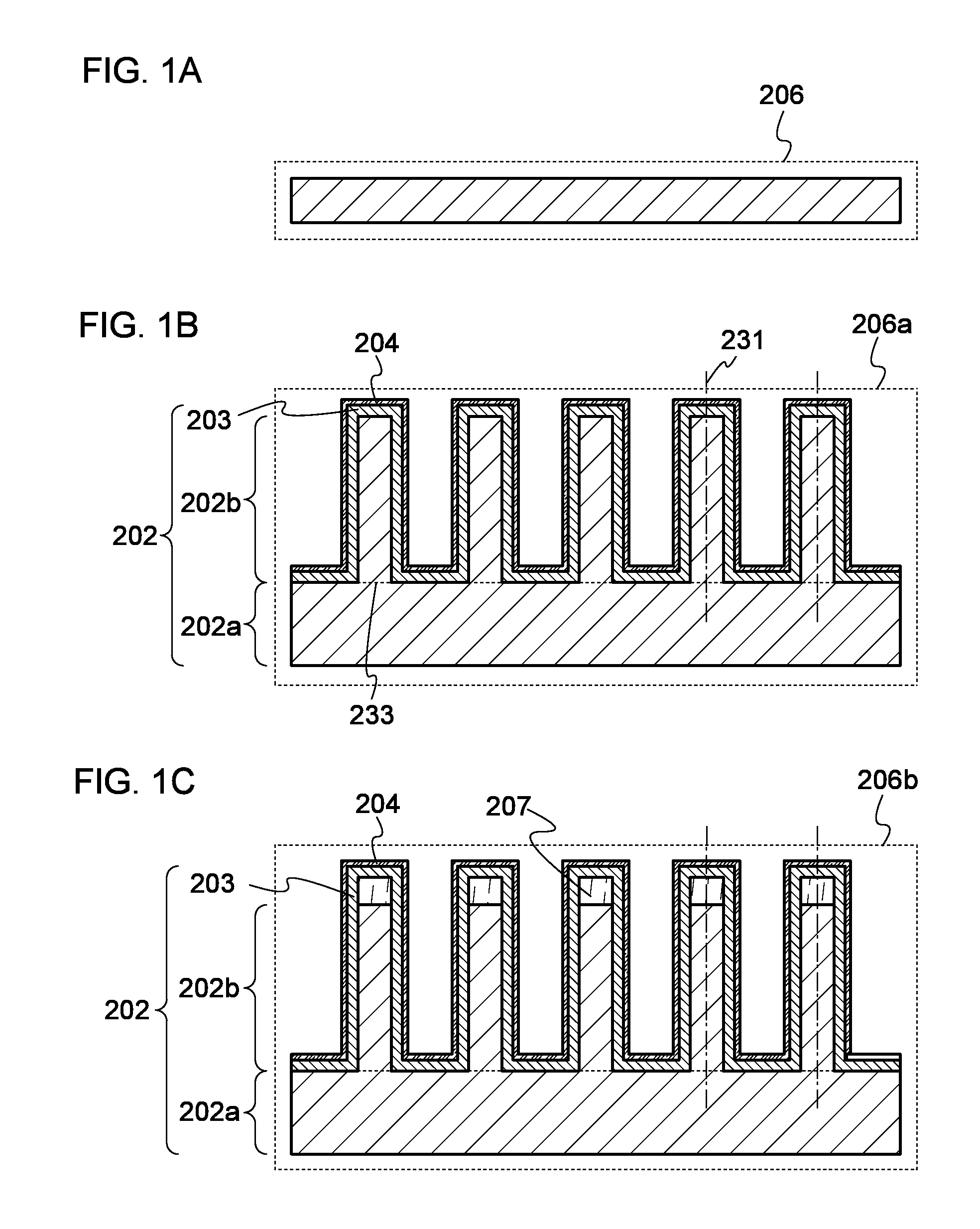
[0046]In this embodiment, a structure of a negative electrode of a power storage device which is less deteriorated through charge / discharge and has excellent cycle characteristics and a manufacturing method thereof will be described with reference to FIGS. 1A to 1C, FIGS. 2A to 2D, FIGS. 3A to 3D, and FIGS. 4A to 4C.

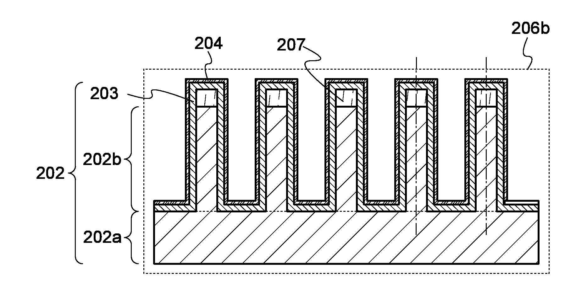
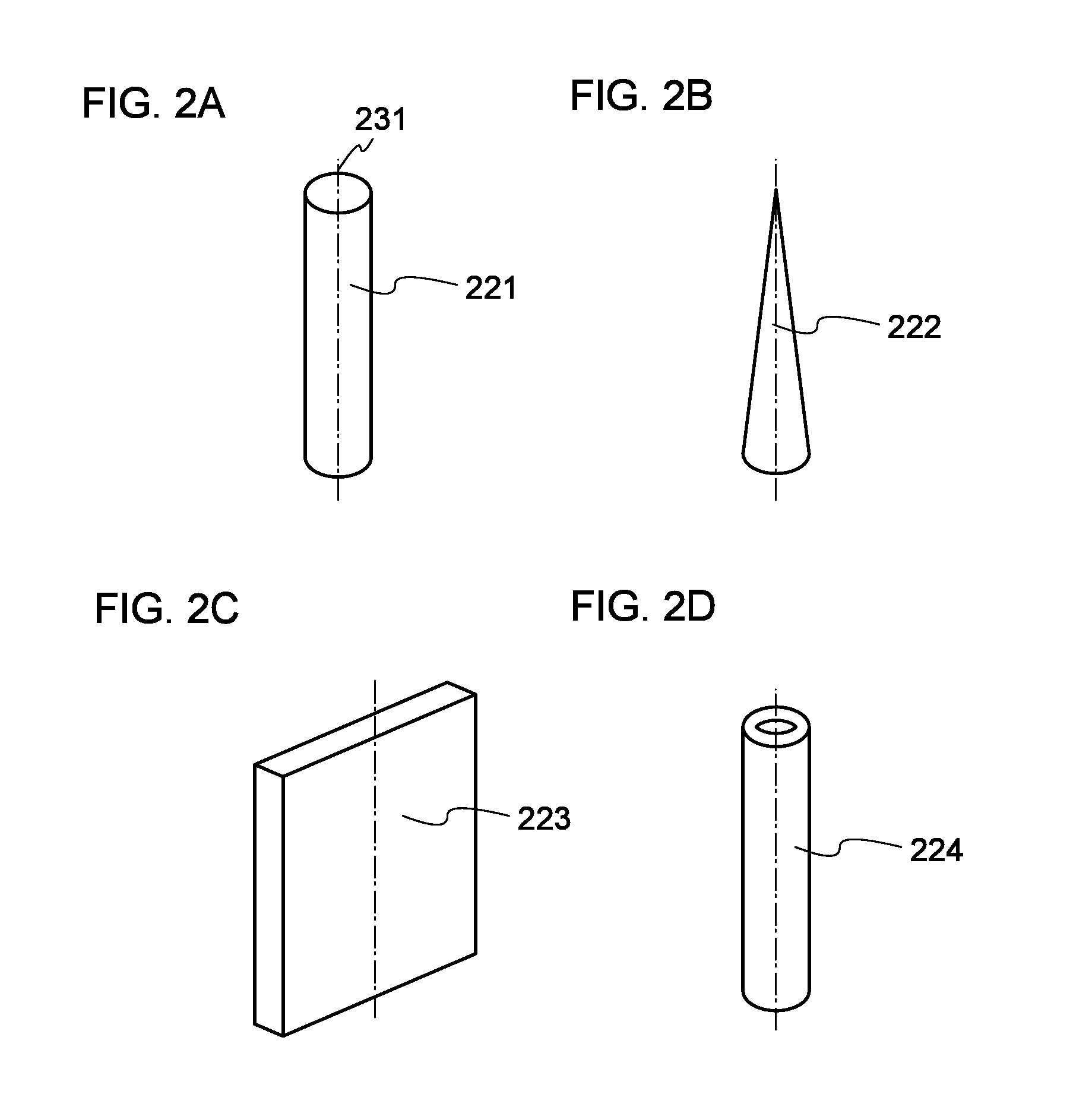
[0047]FIG. 1A is a cross-sectional view of a negative electrode 206 according to an embodiment of the present invention. The negative electrode 206 functions as an active material.

[0048]Note that the active material refers to a material that relates to occlusion and release of carrier ions. An active material layer contains, in addition to the active material, one or more of a conductive additive, a binder, graphene, and the like. Thus, the active material and the active material layer are distinguished from each other.

[0049]A secondary battery in which lithium ions are used as carrier ions is referred to as a lithium-ion secondary battery. In addition, as examples of ca...

embodiment 2

[0114]In this embodiment, a negative electrode having a structure different from that of Embodiment 1 and a method for manufacturing the negative electrode will be described with reference to FIGS. 5A to 5D and FIGS. 6A to 6C. The negative electrode described in this embodiment is different from that of Embodiment 1 in that a current collector is provided.

[0115]FIG. 5A is a cross-sectional view of a negative electrode 216. In the negative electrode 216, an active material layer 215 is provided over a current collector 211.

[0116]A specific structure of the negative electrode 216 will be described with reference to FIGS. 5B to 5D. Typical examples of the active material layer 215 included in the negative electrode 216 are an active material layer 215a, an active material layer 215b, and an active material layer 215c in FIGS. 5B, 5C, and 5D, respectively.

[0117]FIG. 5B is an enlarged cross-sectional view of the current collector 211 and the active material layer 215a. The active materia...

embodiment 3

[0146]In this embodiment, a structure of a power storage device and a method for manufacturing the power storage device will be described.

[0147]First, a positive electrode and a formation method thereof will be described.

[0148]FIG. 7A is a cross-sectional view of a positive electrode 311. In the positive electrode 311, a positive electrode active material layer 309 is formed over a positive electrode current collector 307.

[0149]As the positive electrode current collector 307, a material having high conductivity such as platinum, aluminum, copper, titanium, or stainless steel can be used.

[0150]The positive electrode current collector 307 can have a foil-like shape, a plate-like shape, a net-like shape, or the like as appropriate.

[0151]The positive electrode active material layer 309 can be formed using a lithium compound such as LiFeO2, LiCoO2, LiNiO2, or LiMn2O4, or V2O5, Cr2O5, MnO2, or the like as a material.

[0152]Alternatively, an olivine-type lithium-containing composite oxide (...


PUM

PropertyMeasurementUnit
angleaaaaaaaaaa
angleaaaaaaaaaa
widthaaaaaaaaaa

Abstract

A power storage device in which charge capacity and discharge capacity are high and deterioration in battery characteristics due to charge/discharge is small is provided. A power storage device in which charge capacity and discharge capacity are high and output characteristics are excellent is provided. A power storage device in which charge capacity and discharge capacity are high and cycle characteristics are excellent is provided. A power storage device includes a negative electrode. The negative electrode includes a current collector, an active material including a plurality of protrusions protruding from the current collector and an outer shell in contact with and attached to surfaces of the plurality of protrusions, and graphene in contact with and attached to the outer shell. Axes of the plurality of protrusions are oriented in the same direction. A common portion may be provided between the current collector and the plurality of protrusions.

Description

BACKGROUND OF THE INVENTION[0001]1. Field of the Invention[0002]The present invention relates to a power storage device and a method for manufacturing the power storage device.[0003]2. Description of the Related Art[0004]In recent years, power storage devices such as lithium-ion secondary batteries, lithium-ion capacitors, and air cells have been developed.[0005]An electrode for the power storage device is manufactured by providing an active material over a surface of a current collector. As a negative electrode active material, a material which can occlude and release ions functioning as carriers (hereinafter referred to as carrier ions), such as carbon or silicon, is used. For example, silicon or phosphorus-doped silicon can occlude about four times as many carrier ions as carbon, and thus has higher theoretical capacity than carbon and is advantageous in increasing the capacity of the power storage device.[0006]However, when the amount of carrier ions which are occluded is increa...

Claims


Application Information

Patent Timeline
Patent Type & Authority Applications(United States)
IPC IPC(8): H01M4/66H01M4/583
CPCH01G11/26Y02E60/13H01G11/70H01M4/134H01M4/366H01M4/587H01M4/624H01M4/625H01M4/667H01M4/70H01M10/052H01M2004/025Y02E60/122Y02T10/7011Y02T10/7022H01G11/36Y02E60/10Y02T10/70
Inventor TAJIMA, RYOTAOSADA, TAKESHI
Owner SEMICON ENERGY LAB CO LTD
Why Eureka
Try Eureka