Wiring substrate and method of manufacturing the same

a technology of wiring substrate and resistor, which is applied in the direction of resistive material coating, metallic pattern materials, metallic material coating process, etc., can solve the problems of reducing the adhesion strength between the laminate (i.e., the conductor portion) and the resistor, and reducing the adhesion strength. , to achieve the effect of preventing the formation of short circuit, reducing the generation of whiskers, and increasing the adhesion strength

Active Publication Date: 2013-03-28
NGK SPARK PLUG CO LTD
View PDF3 Cites 4 Cited by
  • Summary
  • Abstract
  • Description
  • Claims
  • Application Information

AI Technical Summary

Benefits of technology

[0011]An object of the present invention is to solve the above-mentioned problem involved in the manufacture of a wiring substrate which has a resistor formed on a substrate, such as a ceramic multilayer wiring substrate, and in which a plurality of wiring layers including film-like conductor portions are formed on the resistor. Specifically, the object of the present invention is to suppress generation of whiskers at the time of formation of the plurality of wiring layers through etching, so as to prevent formation of a short circuit between the plurality of wiring layers and to prevent undercut of the film-like conductor portions of the wiring layers, to thereby increase the adhesion strength between the plurality of wiring layers and the substrate.
[0027]In defining the first-main-face-side wiring layers, the first grounding metal layer and the first conductor layer which constitute the first-main-face-side wiring layers, excluding the portion of the first grounding metal layer to be removed for dividing the first grounding metal layer into two portions, are not exposed to, for example, the etchant. Therefore, it is possible to prevent formation of fibrous foreign objects, called “whiskers,” which have conventionally been formed when these layers are etched, such that the whiskers extend outward. As a result, it is possible to avoid problems, such as a problem that the first-main-face-side wiring layers formed on the resistor are electrically connected with each other via the “whiskers,” which results in formation of a short circuit.
[0028]Also, as described above, the first-main-face-side wiring layers, excluding the portion of the first grounding metal layer to be removed for dividing the first grounding metal layer into two portions, are not exposed to, for example, etchant. Therefore, even when the etchant stagnates, it is possible to prevent anisotropic etching. Therefore, it is possible to prevent excessive etching of a lower portion of each first-main-face-side wiring layer; i.e., a lower portion of the first grounding metal layer or the like, which would otherwise result in formation of an undercut. Accordingly, it is possible to avoid problems, such as a decrease in the adhesion strength between the first-main-face-side wiring layers and the resistor, which results in separation of the first-main-face-side wiring layers from the resistor.
[0030]As described above, according to the present invention, it is possible to solve the problem involved in manufacture of a wiring substrate which has a resistor formed on a substrate, such as a ceramic multilayer wiring substrate, and in which a plurality of wiring layers including film-like conductor portions are formed on the resistor. Specifically, it is possible to suppress generation of whiskers at the time of formation of the plurality of wiring layers through etching, so as to prevent formation of a short circuit between the plurality of wiring layers and to prevent undercut of the film-like conductor portions of the wiring layers, to thereby increase the adhesion strength between the plurality of wiring layers and the substrate.

Problems solved by technology

Such “whiskers” cause various problems.
Thus, particularly in the case where each of the conductor portions is formed of the above-mentioned film-like laminate, the etching may proceed excessively at a lower portion of the film-like laminate such that an undercut is formed.
In such a case, the adhesion strength between the laminate (i.e., the conductor portion) and the resistor decreases, and various problems may occur.

Method used


Image

  • Wiring substrate and method of manufacturing the same
  • Wiring substrate and method of manufacturing the same
  • Wiring substrate and method of manufacturing the same

Examples


first embodiment

Wiring Substrate

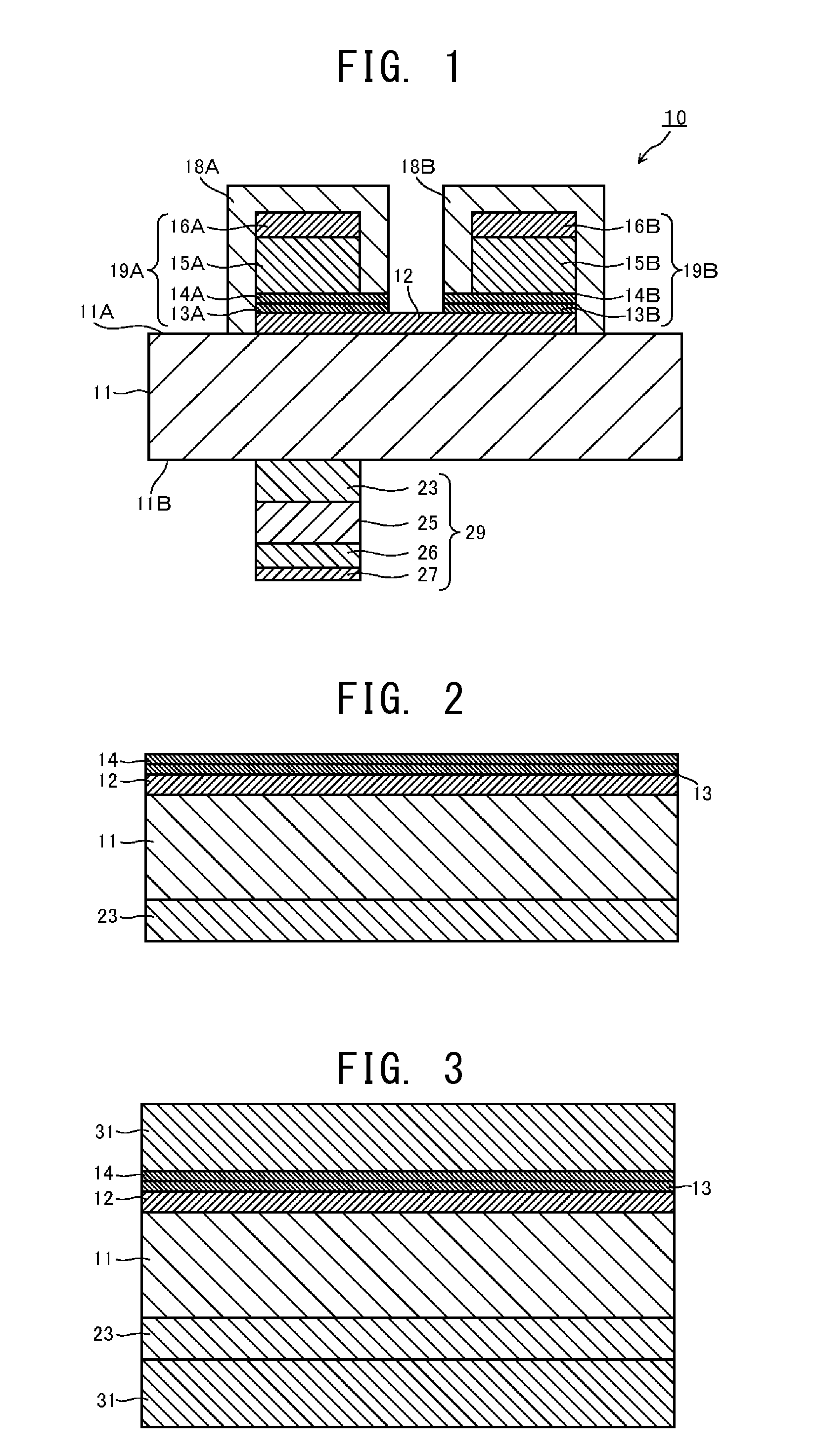
[0052]FIG. 1 is a sectional view schematically showing the structure of a wiring substrate according to the present embodiment. As shown in FIG. 1, a wiring substrate 10 of the present embodiment includes a substrate main body 11 and a film-like resistor 12 formed of, for example, Ta2N. The resistor 12 is formed on a first main face 11A of the substrate main body 11 such that the resistor 12 is electrically connected to an internal wiring layer (e.g., a via) formed in the substrate main body 11. The substrate main body 11 may be formed of, for example, a ceramic multilayer wiring substrate.

[0053]A first-main-face-side wiring layer 19A (a stack of layers collectively called “wiring layer 19A”) is provided on the resistor 12. The first-main-face-side wiring layer 19A is constituted by sequentially forming a first portion 13A of a first grounding metal lower layer formed of, for example, Ti and having a thickness of 0.2 μm, a first portion 14A of a first grounding metal...

second embodiment

Wiring Substrate

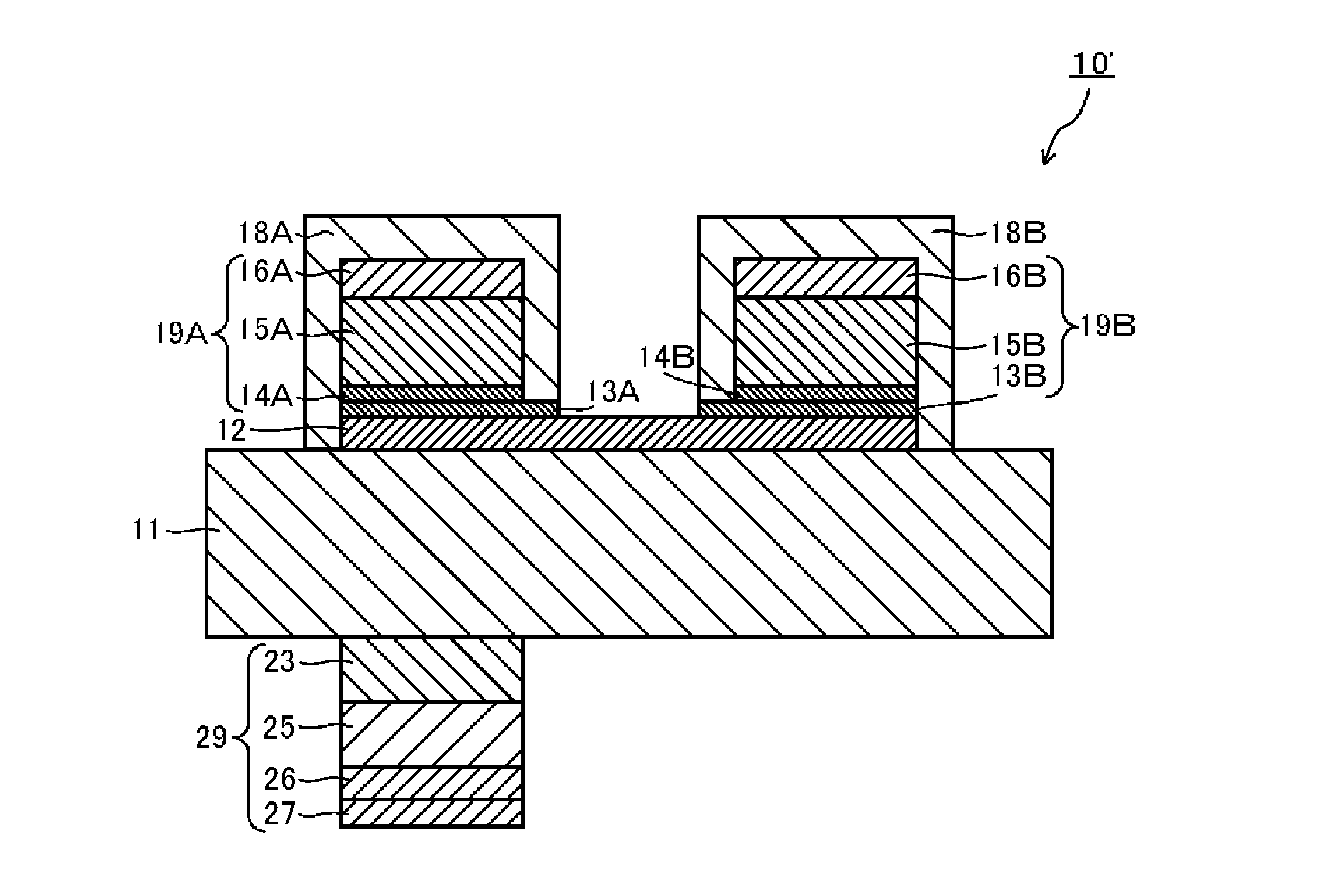
[0091]FIG. 18 is a sectional view schematically showing the structure of a wiring substrate according to the present embodiment. Notably, structural elements similar or identical to those of the wiring substrate 10 shown in FIG. 1 are denoted by the same reference numerals.

[0092]A wiring substrate 10′ of the present embodiment differs from the wiring substrate 10 of the first embodiment in that the conductive covering layers 18A and 18B are formed on the first main face 11A of the substrate main body 11 such that the conductive covering layers 18A and 18B cover the mutually facing side surfaces of the first-main-face-side wiring layers 19A and 19B. Specifically, the conductive covering layer 18A covers the side surface of the first portion 14A of the first grounding metal upper layer of the first-main-face-side wiring layer 19A, which side surface faces the first-main-face-side wiring layer 19B, and the conductive covering layer 18B covers the side surface of the sec...


PUM

PropertyMeasurementUnit
thicknessaaaaaaaaaa
thicknessaaaaaaaaaa
thicknessaaaaaaaaaa

Abstract

A wiring substrate includes a substrate main body having a first main face and a second main face opposite the first main face; a resistor formed on the first main face; a plurality of first-main-face-side wiring layers which are each formed on the resistor and which each include a grounding metal layer formed of a metal having a resistance lower than that of the resistor and a conductor layer formed on the grounding metal layer; a second-main-face-side wiring layer formed on the second main face; and a via which is formed in the substrate main body and which establishes electrical connectivity between the first-main-face-side wiring layers and the second-main-face-side wiring layer. The wiring substrate further includes a conductive covering layer which covers an upper surface and substantially covers the side surfaces of each of the first-main-face-side wiring layers.

Description

CROSS REFERENCE TO RELATED APPLICATIONS[0001]The present application claims priority from Japanese Patent Application No. 2011-207478, which was filed on Sep. 22, 2011, the disclosure of which is herein incorporated by reference in its entirety.BACKGROUND OF THE INVENTION[0002]1. Field of the Invention[0003]The present invention relates to a wiring substrate having a resistor and to a method of manufacturing the same.[0004]2. Description of Related Art[0005]In recent years, a resistor is formed on a main face of a ceramic multilayer wiring substrate by means of sputtering or the like so as to realize impedance matching of signal wiring of the ceramic multilayer wiring substrate. The resistor suppresses reflection of signals, and prevents generation of noise and deterioration of signals.[0006]Meanwhile, a wiring layer (as used herein, “a wiring layer” refers to a stack of conductive layers) is provided on the resistor. This wiring layer includes two or more film-like conductor portio...

Claims


Application Information

Patent Timeline
Patent Type & Authority Applications(United States)
IPC IPC(8): H05K1/16H05K1/09H05K3/10H05K1/11
CPCH05K1/0246H05K1/0251H05K2201/0317H05K1/167H05K3/242H05K1/0306H01C7/00H05K1/16
Inventor SUZUKI, KENJIKITO, MASANORIOTSUKA, YUMAKAMIYA, HISAYOSHITANABASHI, TSUYOSHI
Owner NGK SPARK PLUG CO LTD
Why Eureka
Try Eureka