

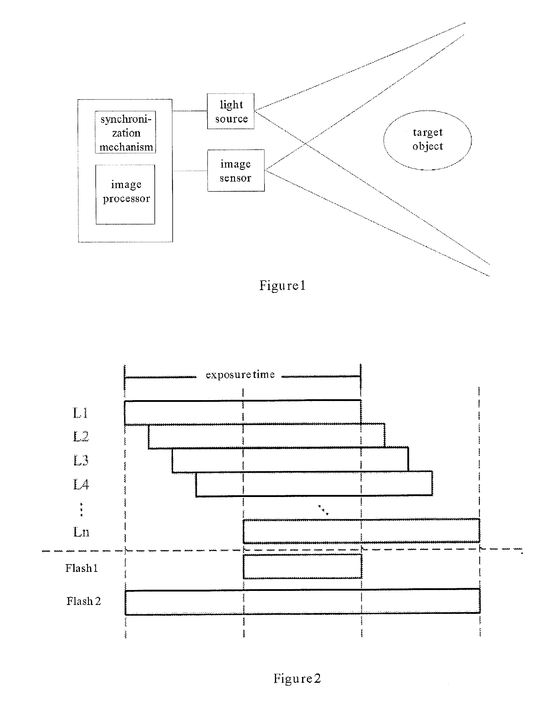
CMOS Image Sensor, Timing Control Method and Exposure Method Thereof
a timing control and image sensor technology, applied in the field of image sensors, can solve the problems of poor real-time performance of image acquisition and low utilization efficiency of light source energy, and achieve the effects of improving light source energy utilization efficiency, facilitating various exposure methods of cmos image sensors, and controlling more flexibly
- Summary
- Abstract
- Description
- Claims
- Application Information
AI Technical Summary
Benefits of technology
Problems solved by technology
Method used
Image

Examples
first embodiment
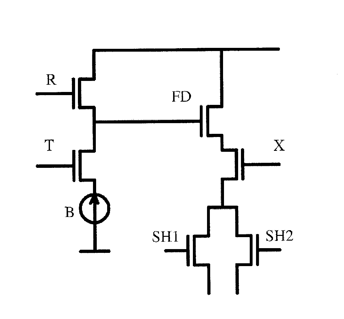
[0097]Reference is now made to FIG. 8, which is a flowchart of the exposure method of the CMOS image sensor according to the present invention. As shown in FIG. 8, the exposure method of the present embodiment includes the following steps A0-A5.
[0098]First, in step A0, the CMOS image sensor is divided into a plurality of sub-arrays each composed of the same number of pixel rows.
[0099]Subsequently, in step A1, the first sub-array is selected as the current sub-array for exposing.
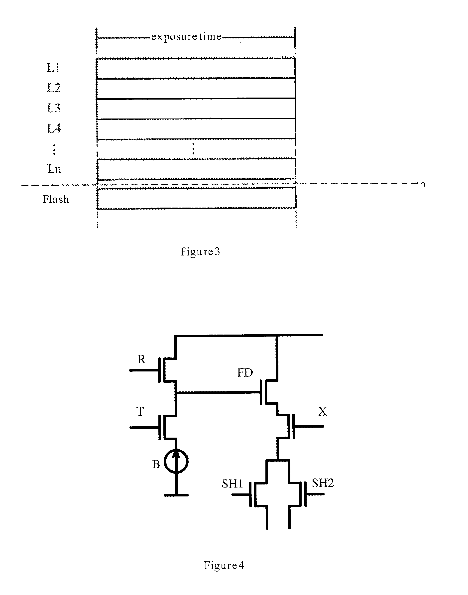
[0100]Subsequently, in step A2, each pixel row in the current sub-array for exposing is controlled to be synchronously exposed and to output data, in the first light source state and the second light source state, respectively. Step A2 further includes: step A21 for controlling, in the first light source state, each pixel row in the current sub-array for exposing to undergo the first synchronous exposure, and controlling the pixel row to sequentially output the data to a first frame buffer until the data outp...
second embodiment
[0109]Reference is now made to FIG. 11, which is a schematic diagram of the process of the exposure method of the CMOS image sensor according to present invention. First, in step A′0, the CMOS image sensor is divided into a plurality of sub-arrays each composed of the same number of pixel rows.
[0110]Subsequently, in step A′1, the last sub-array is selected as the current sub-array for exposing.
[0111]Subsequently, in step A′2, each pixel row in the current sub-array for exposing is controlled to be synchronously exposed and to output the data, in the first light source state and the second light source state, respectively. Step A′2 further includes: step A′21 for controlling, in the first light source state, each pixel row in the current sub-array for exposing to undergo a first synchronous exposure, and controlling the pixel row to sequentially output the data to a first frame buffer until the data outputs by all pixel rows in the current sub-array for exposing are completed; and st...
third embodiment
[0116]Reference is now made to FIG. 13, which is a flowchart of the exposure method of the CMOS image sensor according to the present invention. In this method, the CMOS image sensor is also divided into a plurality of sub-arrays for the exposing. As shown in FIG. 13, the exposure method of the present embodiment includes the following steps B0-B5.
[0117]First, in B0 step, the CMOS image sensor is divided into a plurality of sub-arrays each composed of the same number of pixel rows.
[0118]Subsequently, in step B1, the first sub-array is selected as the current sub-array for exposing.
[0119]Subsequently, step B2 specifically including step B21 and step B22 as shown in FIG. 13 is performed. In step B21, in the first light source state, each pixel row in the current sub-array for exposing is controlled to undergo the first synchronous exposure, and then the data of the lower half of the pixel rows in the current sub-array for exposing are firstly outputted to the first frame buffer. In st...
PUM
 Abstract
Description
Claims
Application Information