Thin film transistor fabricating method
- Summary
- Abstract
- Description
- Claims
- Application Information
AI Technical Summary
Benefits of technology
Problems solved by technology
Method used
Image

Examples
Embodiment Construction
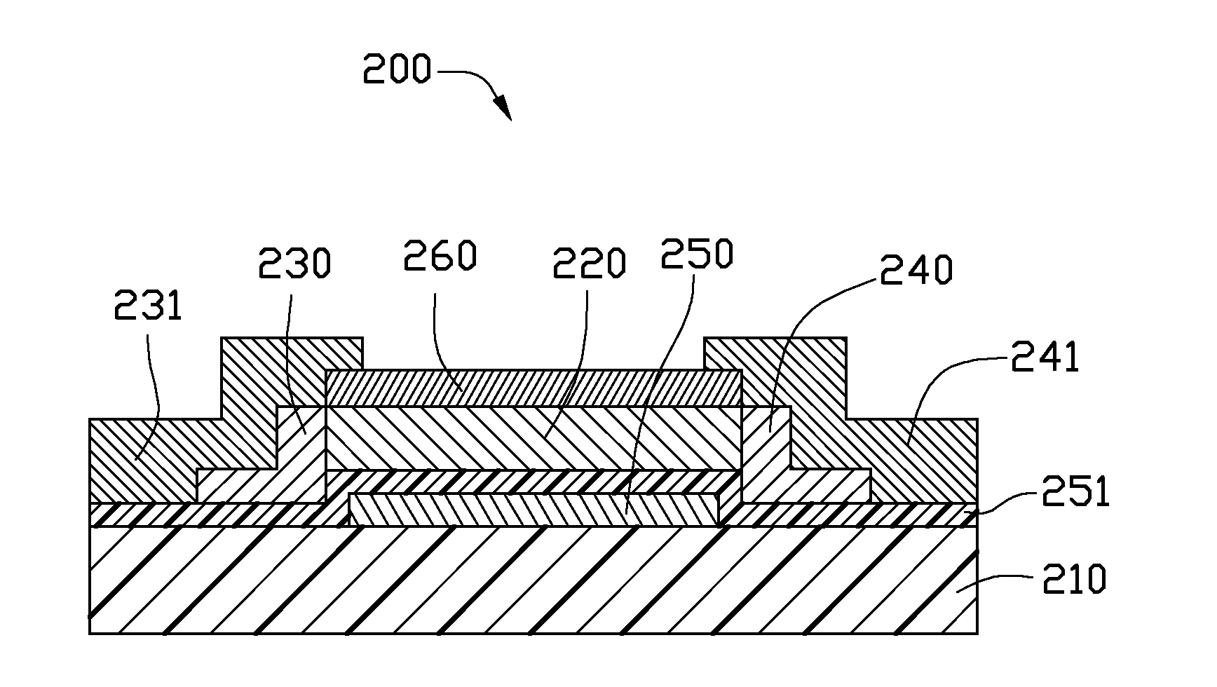
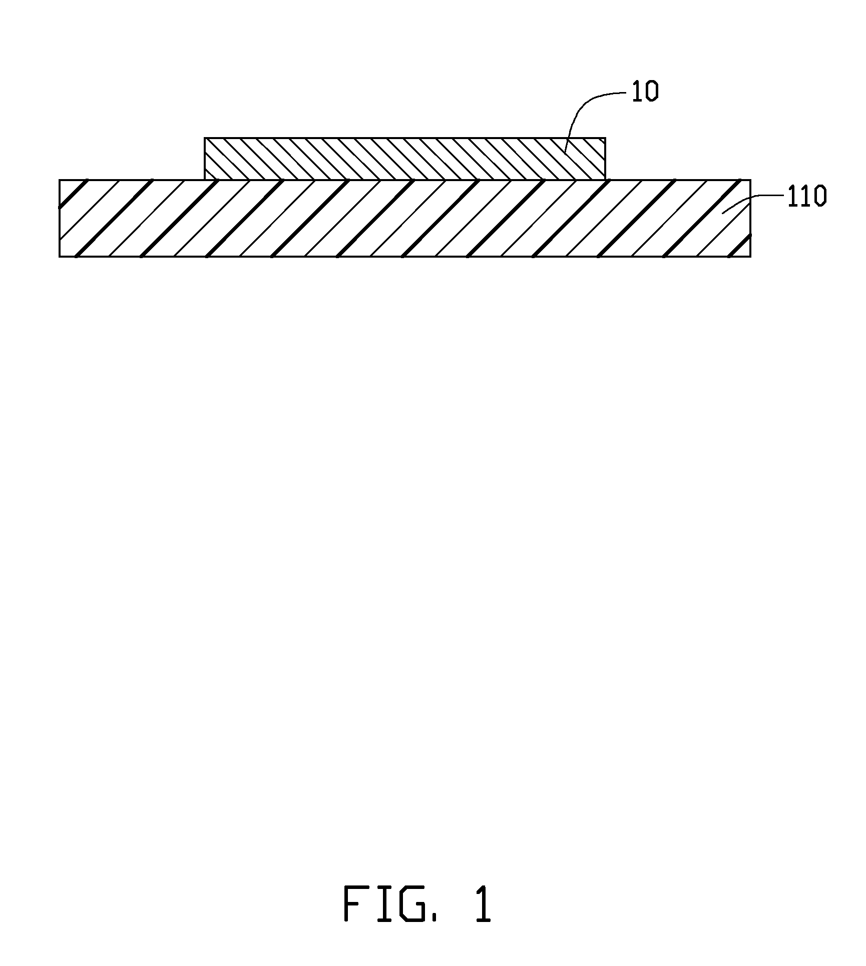
[0008]Embodiments of a method for fabricating thin film transistors will now be described in detail below and with reference to the drawings.
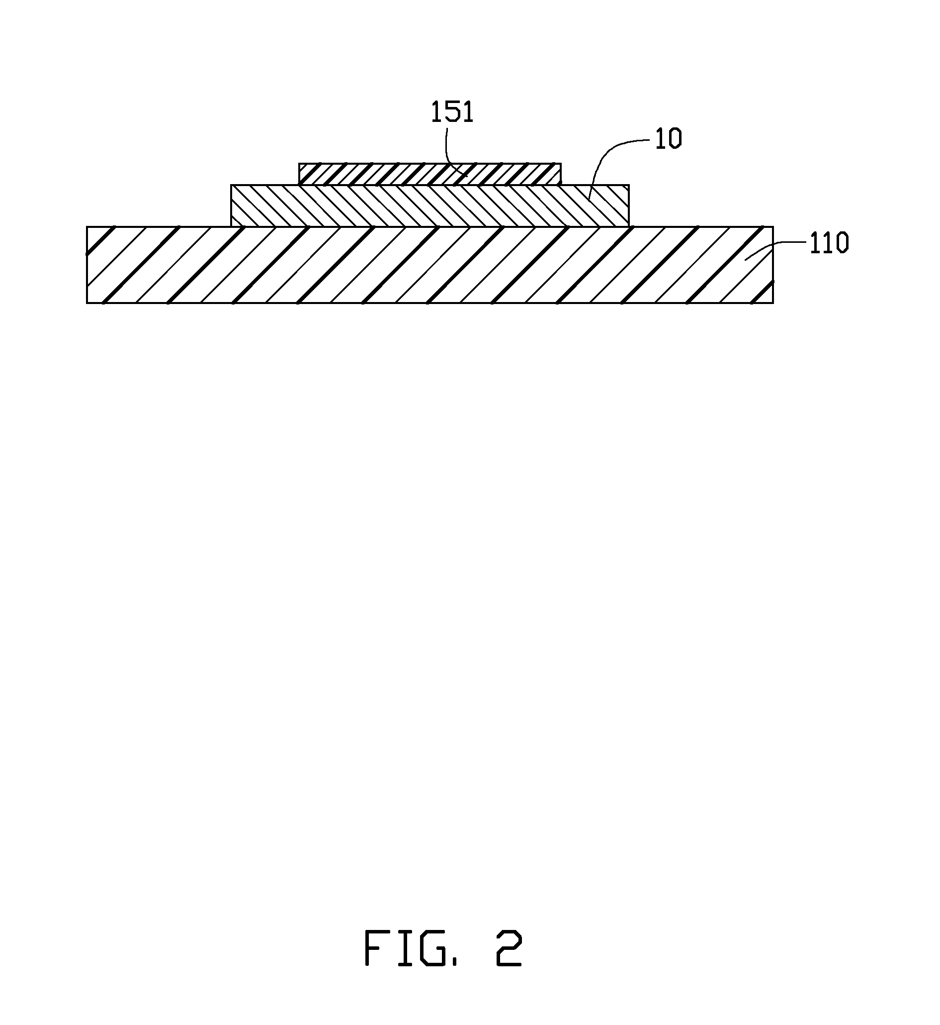
[0009]Referring to FIG. 1, an oxide semiconductor layer 10 is formed on a substrate 110. The substrate 110 is made of a material selected from a group consisting of glass, quartz, silicone, polycarbonate, polymethyl methacrylate, and metal foil. The oxide semiconductor layer 10 is made of a material selected from a group consisting of IGZO, ZnO, TiOx, GTO, GZO, AZO, IZO, ITO, ATO, In2O3, and SnO2.
[0010]Referring to FIG. 2, a gate insulating layer 151 is formed on part of an upper surface of the oxide semiconductor layer 10. In this embodiment, the gate insulating layer 151 is positioned at a central region of the upper surface of the oxide semiconductor layer 10. The gate insulating layer 151 is made of a material selected from a group consisting of SiOx, SiNx, and SioNx.
[0011]Referring to FIG. 3, with the gate insulating layer 151 functioning ...
PUM
 Abstract
Description
Claims
Application Information
 - R&D Engineer
- R&D Manager
- IP Professional
- Industry Leading Data Capabilities
- Powerful AI technology
- Patent DNA Extraction
Browse by: Latest US Patents, China's latest patents, Technical Efficacy Thesaurus, Application Domain, Technology Topic.
© 2024 PatSnap. All rights reserved.Legal|Privacy policy|Modern Slavery Act Transparency Statement|Sitemap