Display Drives Circuits and Techniques

a technology of display drive and circuit, applied in the direction of static indicating devices, electrical appliances, instruments, etc., can solve the problems of difficult to predict how bright a pixel will appear when driven by a given voltage, increase the area of the pixel driver circuit, and reduce flicker. , the effect of increasing the lifetim

a technology of display drive and circuit, applied in the direction of static indicating devices, electrical appliances, instruments, etc., can solve the problems of difficult to predict how bright a pixel will appear when driven by a given voltage, increase the area of the pixel driver circuit, and reduce flicker. , the effect of increasing the lifetim

US20130082912A1Inactive Publication Date: 2013-04-04CAMBRIDGE DISPLAY TECH LTD

Image

  • Display Drives Circuits and Techniques
  • Display Drives Circuits and Techniques
  • Display Drives Circuits and Techniques

Examples


Embodiment Construction

Pixel Driver Architecture

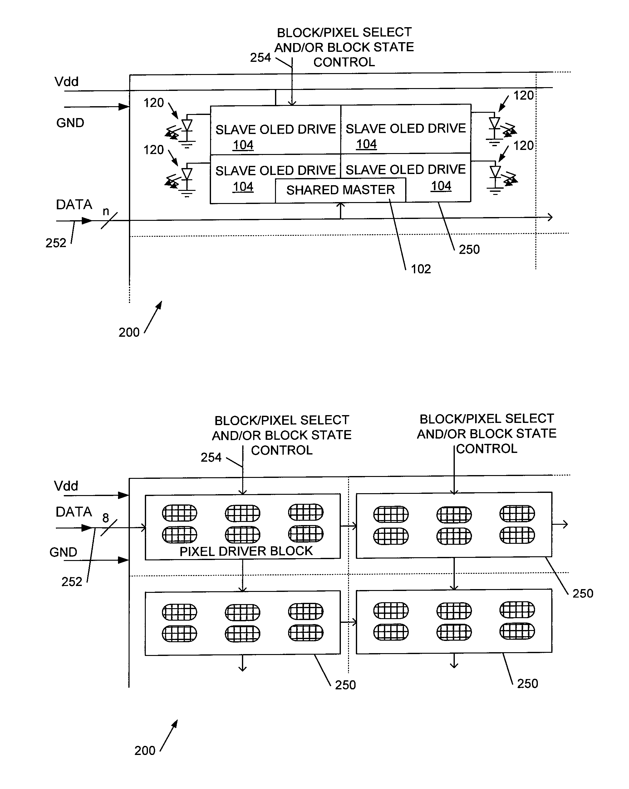
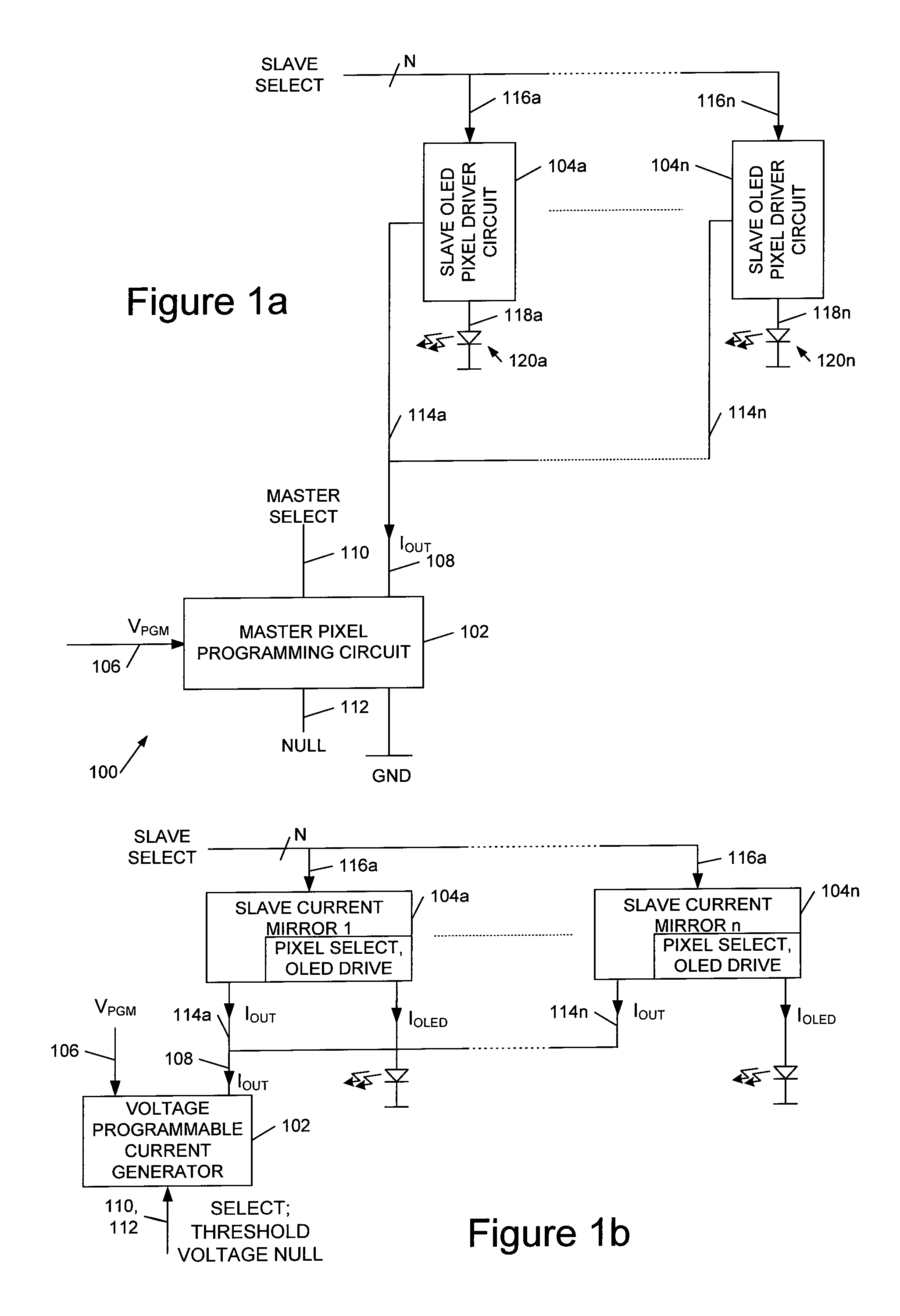
[0028]Referring to FIG. 1a, this shows an embodiment of a pixel driver architecture 100 according to the invention comprising a voltage-programmed master pixel programming circuit 102 coupled to a plurality of current-programmed slave pixel driver circuits 104a-n. The master circuit 102 has a voltage programming line 106 to receive a programming voltage and provides a programmed current on a current output line 108 controlled by the input voltage. Optionally the master pixel programme circuit also includes a select line 110 and a null control line 112, the latter for nulling a threshold voltage on an output transistor of the circuits. Each slave pixel driver circuit has a current programming input line 114a-n and a respective select line 116a-n and has an OLED drive output 118a-n to drive a respective OLED 120a-n.

[0029]FIG. 1b shows an example of the circuit of FIG. 1a in which each slave pixel driver circuit is implemented by a current mirror which, in emb...


PUM


Abstract

A pixel driver architecture for an active matrix OLED display, the pixel driver architecture comprising a voltage-programmed master pixel programming circuit, and a first plurality of current-programmed slave pixel driver circuits, each coupled to said master pixel programming circuit.

Description

FIELD OF THE INVENTION[0001]This invention relates to improved techniques for driving organic light emitting diodes (OLED) displays.BACKGROUND OF THE INVENTION[0002]It is known to drive an OLED display using an active matrix arrangement in which individual pixels of the display are activated by an associated thin film transistor (TFT). The brightness of an OLED pixel of such a display may be programmed by either a voltage or a current. (In this specification references to ‘pixels’ are to be interpreted as including different colored sub-pixels of a color display). In either case a typically memory element is associated with each pixel so that the data written to a pixel is retained while other pixels are addressed. Generally this is achieved by a storage capacitor which stores a voltage set on the gate of a driver transistor, which in turn dictates the current through the OLED pixel. However the voltage on the gate of the TFT driver transistor, and hence the OLED current, may be pro...

Claims


Application Information

Patent Timeline
04 Apr 2013
Publication
US20130082912A1
IPC
G09G3/32
CPC
H04N13/0438; H04N2213/001; G09G2320/045; G09G3/3283; G09G2320/0233; G09G3/2088; H04N13/341; G09G3/3225
Inventors
SMITH, EUAN C.