

Method for Forming Single-Phase Multi-Element Film by PEALD
a multi-element film, single-phase technology, applied in the direction of coatings, chemical vapor deposition coatings, metallic material coating processes, etc., can solve the problems of insufficient etch selectivity of mono-element si-based insulation films, base substrates or photoresists are vulnerable to deformation, and the operation is complicated and requires more steps
- Summary
- Abstract
- Description
- Claims
- Application Information
AI Technical Summary
Benefits of technology
Problems solved by technology
Method used
Image

Examples
example 1
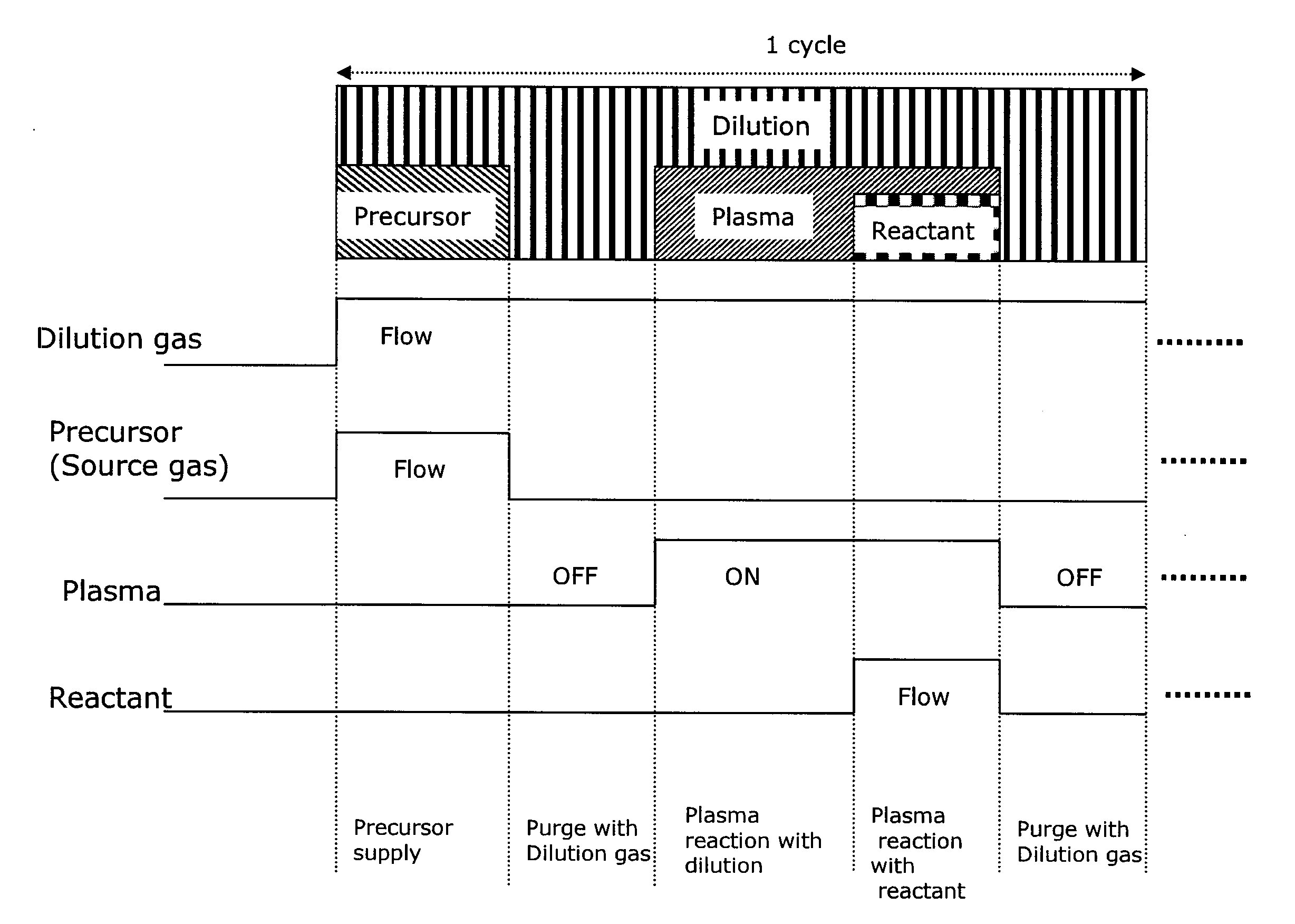
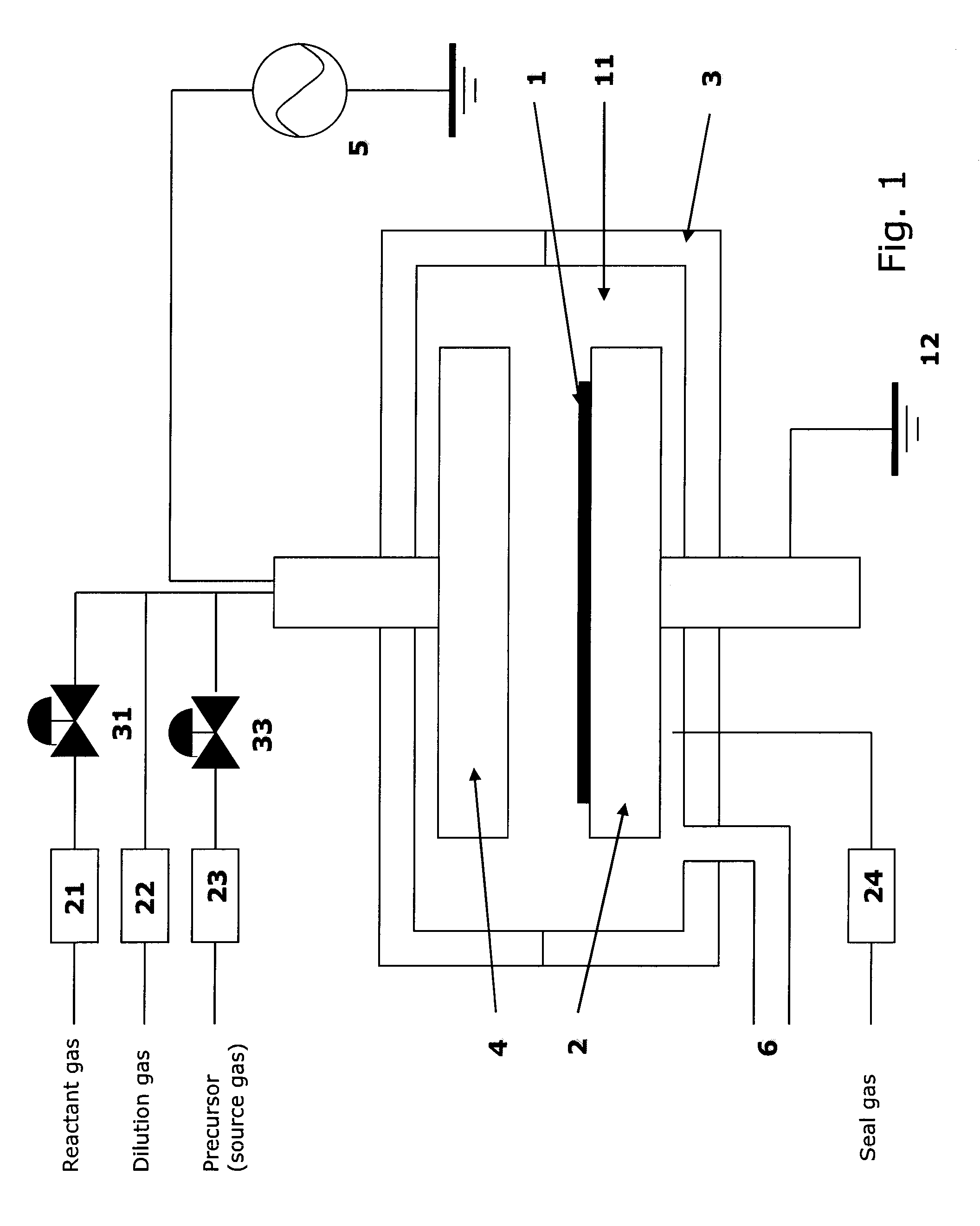
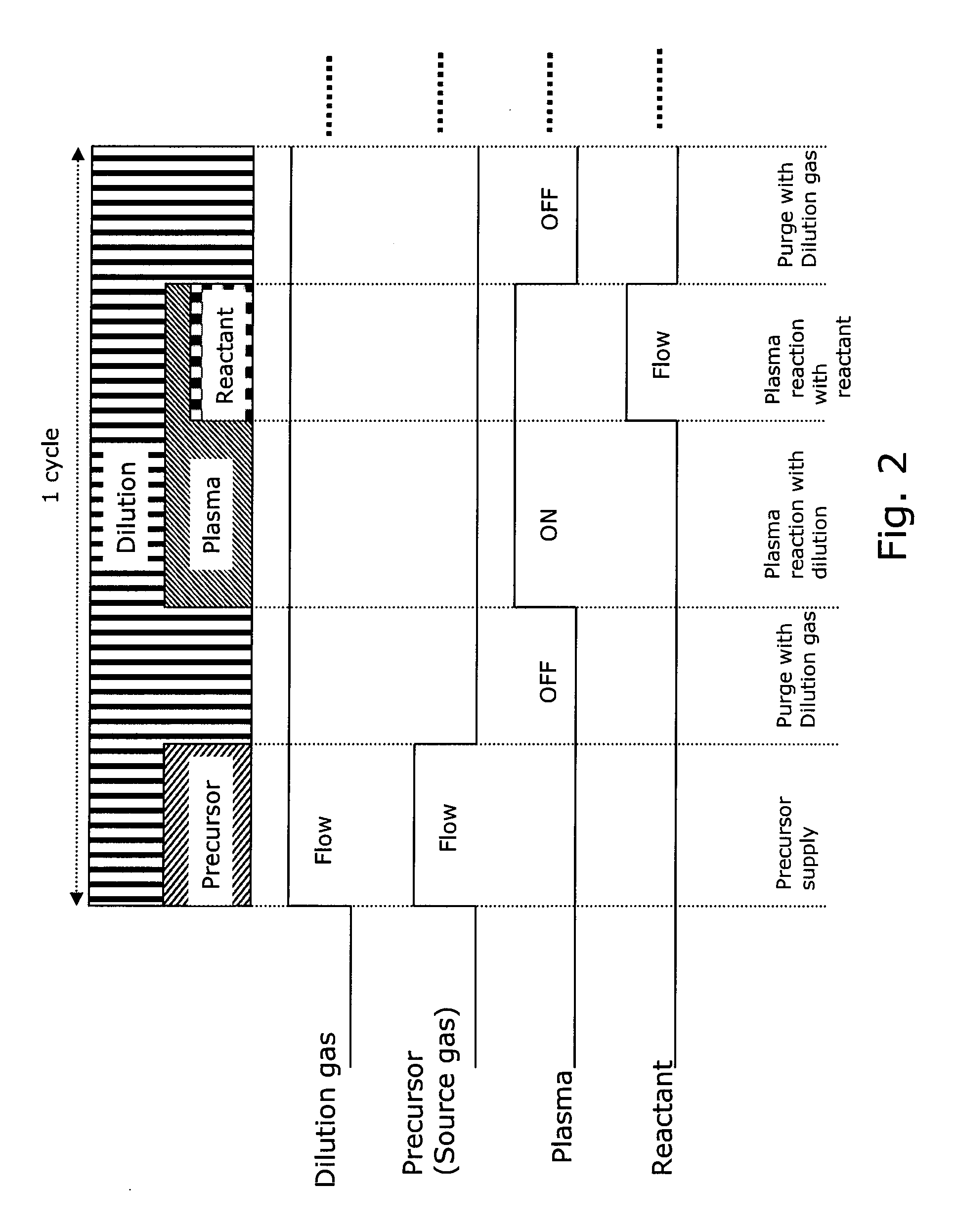
[0056]A dielectric multi-element SiOX film was formed on a 300-mm substrate under the conditions shown below using the sequence illustrated in FIG. 2 and the PEALD apparatus illustrated in FIG. 1. In this example, X was C and N.
[0057]The length of one cycle: 3.1 sec to 4.1 sec
[0058]Precursor: BDEAS: 500 sccm to 1,000 sccm
[0059]Dilution gas: He: 2000 sccm
[0060]Reactant gas: O2: 30 sccm
[0061]Seal gas: He: 500 sccm
[0062]Substrate temperature: 100° C.
[0063]Pressure: 230 Pa
[0064]High frequency RF power (a frequency of 13.56 MHz): 0.08 W / cm2
[0065]Precursor supply pulse duration: 1.5 sec
[0066]Purge time: 0.3 sec
[0067]The total duration of dilution gas plasma and reactant gas plasma: 1.0 sec
[0068]The number of cycles: 600 times
[0069]The thickness of the film: 10 nm to 20 nm
[0070]The duration of reactant gas plasma was changed from 0 sec to 1.0 sec while maintaining the total duration of dilution gas plasma and reactant gas plasma, 1.0 sec. The refractive index at 633 nm of each resultant f...
example 2
[0072]A dielectric multi-element SiCON film was formed on a 300-mm substrate under the conditions shown below using the sequence illustrated in FIG. 2 and the PEALD apparatus illustrated in FIG. 1.
[0073]The length of one cycle: 2.5 sec
[0074]Precursor: BDEAS: 500 sccm
[0075]Dilution gas: Ar, He: 1000 sccm
[0076]Reactant gas: O2: 40 sccm at maximum
[0077]Seal gas: He: 500 sccm
[0078]Substrate temperature: 50° C.
[0079]Pressure: 200 to 300 Pa
[0080]High frequency RF power (a frequency of 13.56 MHz): 0.07 W / cm2
[0081]Precursor supply pulse duration: 0.5 sec
[0082]Purge time: 0.3 sec
[0083]The duration of dilution gas plasma: 1.0 sec
[0084]The duration of reactant gas plasma: 0.4 sec at maximum
[0085]The number of cycles: 100 times
[0086]The thickness of the film: 10 nm
[0087]After the target multi-element SiCON film was obtained, the composition of the resultant film was analyzed by XPS (Narrow Scan Overlay), and the result is shown in the table below. Since the film was thin, the composition was a...
PUM
| Property | Measurement | Unit |
|---|---|---|
| RI | aaaaa | aaaaa |
| pressure | aaaaa | aaaaa |
| pressure | aaaaa | aaaaa |
Abstract
Description
Claims
Application Information