Method of Fabricating Al2O3 Thin Film Layer

a thin film layer and al2o3 technology, applied in the field of al2o3 thin film, can solve the problems of increasing the price of fossil fuel, increasing the cost of fossil fuel, and rapid shortening of earth storage, and achieve the effect of simple, fast and single procedur

Inactive Publication Date: 2013-04-04
INST NUCLEAR ENERGY RES ROCAEC
View PDF0 Cites 5 Cited by
  • Summary
  • Abstract
  • Description
  • Claims
  • Application Information

AI Technical Summary

Benefits of technology

[0009]The main purpose of the present invention is to fabricate an Al2O3 thin film layer through a simple, fast and single procedure in an environment having a normal atmospheric pressure and a low temperature for obtaining both effects of chemical passivation and field effect passivation.

Problems solved by technology

Fossil fuel is thus greatly consumed and its price is getting higher and higher while its storage on earth is rapidly running short.
At the same time, a great pollution is thus formed to danger human's life owing to the global warming and abnormal weather.
However, after the nuclear catastrophes happened in Three-Miles Island, Fukushima, etc., people start to be worry about the safety issue of nuclear energy.
Yet, this method is not applicable in industrial manufacture.
However, the SiNx thin film has a high density of fixed positive charge and so is not applicable on a back surface of the solar cell having a p-type substrate.
Yet, these methods require vacuum environment, not to mention the deposition velocity slower than 2 nanometers per minute (nm / min) for ALD, and are thus not fit to be used in the industrial manufacture of solar cells.
The above prior arts do not meet the requirements concerning cost and efficiency.
Hence, the prior arts do not fulfill all users' requests on actual use.

Method used


Image

  • Method of Fabricating Al2O3 Thin Film Layer
  • Method of Fabricating Al2O3 Thin Film Layer
  • Method of Fabricating Al2O3 Thin Film Layer

Examples


Embodiment Construction

[0017]The following description of the preferred embodiment is provided to understand the features and the structures of the present invention.

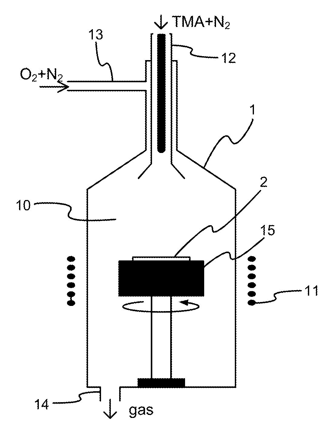
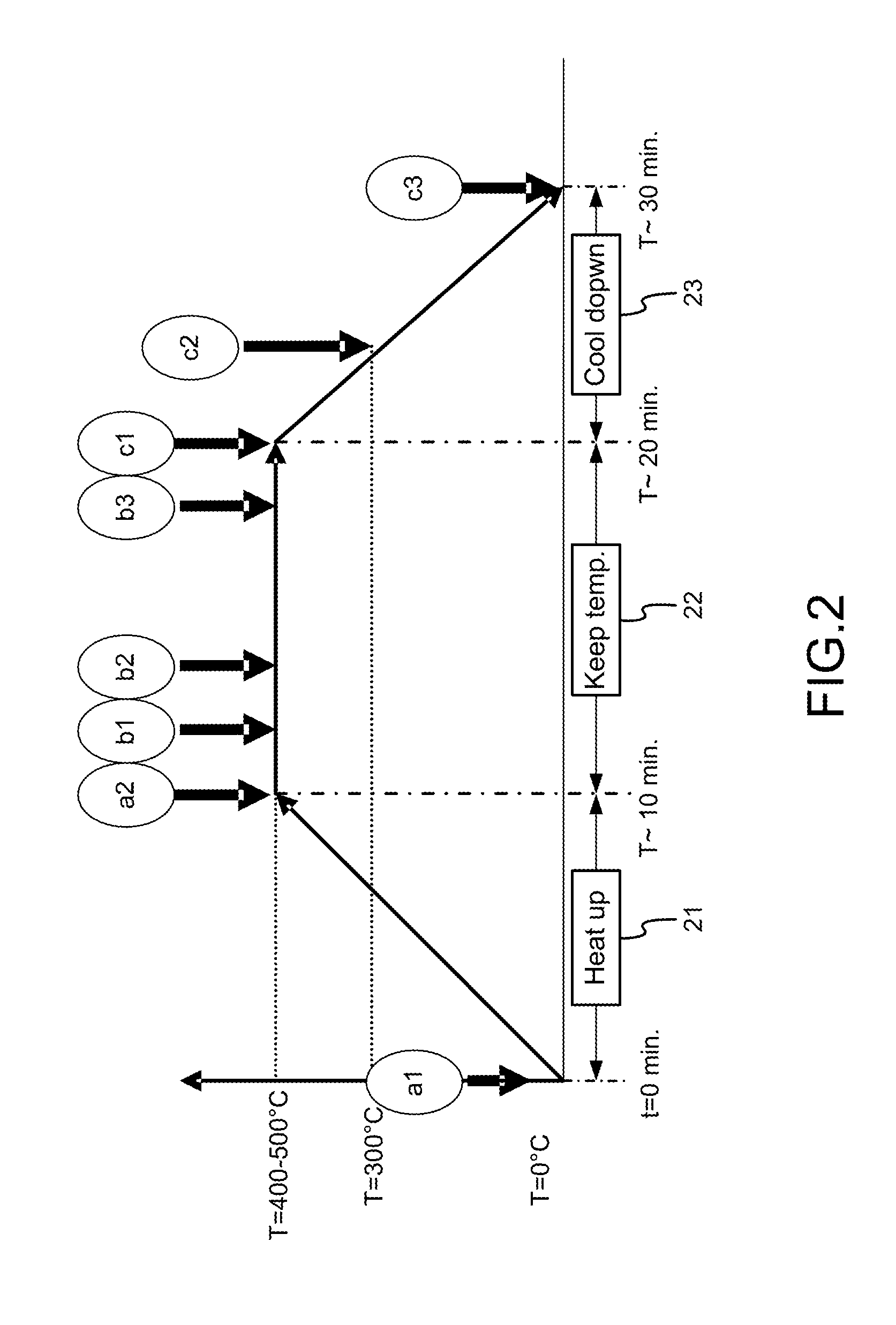
[0018]Please refer to FIG. 1 and FIG. 2, which are a structural view showing a chamber for APCVD; and a view showing a temperature-time curve during fabricating an Al2O3 thin film layer. As shown in the figures, the present invention is a method of fabricating an Al2O3 thin film layer, comprising the following steps:

[0019](a) Heating up 21: A silicon wafer 2 is obtained to be put into a reaction chamber 10 for atmospheric pressure chemical vapor deposition (APCVD) 1 with nitrogen gas flown in. Then, a power source, like a radiofrequency coil 11, is turned on to heat up to a temperature; and, then, heating is stopped at the temperature to obtain a native oxide layer of SiO2 on a surface of the silicon wafer 2 after heat balance is achieved. Therein, the silicon wafer 2 is a p-type or n-type silicon wafer; the silicon wafer 2 has a purity betwe...


PUM

PropertyMeasurementUnit
thicknessaaaaaaaaaa
thicknessaaaaaaaaaa
velocityaaaaaaaaaa

Abstract

An Al2O3 thin film layer is fabricated. Atmospheric pressure chemical vapor deposition (APCVD) is processed in a normal atmospheric pressure and a low temperature. On a surface of a p-type or n-type silicon crystal wafer having a purity between 5N (99.999%) and 9N (99.9999999%), the Al2O3 thin film layer is deposited and fabricated. The deposition and fabrication are done to obtain chemical passivation and field effect passivation. In this way, the present invention can be applied in solar cells and other photoelectric devices with reduced leakage of surface currents and improved photoelectric conversion.

Description

TECHNICAL FIELD OF THE INVENTION[0001]The present invention relates to Al2O3 thin film; more particularly, relates to fabricating an Al2O3 thin film layer through a simple, fast and single procedure in an environment having a normal atmospheric pressure and a low temperature to obtain both effects of chemical passivation and field effect passivation.DESCRIPTION OF THE RELATED ARTS[0002]Following the increase in population, the development in civilization and the demands for a better life, power needs are increasing day by day. Fossil fuel is thus greatly consumed and its price is getting higher and higher while its storage on earth is rapidly running short. At the same time, a great pollution is thus formed to danger human's life owing to the global warming and abnormal weather.[0003]Alternative energies can be the solutions. They can be divided into two categories: solar-originated energies and non-solar-originated energies. Solar-originated energies include energies from wind, tid...

Claims


Application Information

Patent Timeline
Patent Type & Authority Applications(United States)
IPC IPC(8): H01L21/31
CPCC23C16/403H01L31/18H01L31/02167Y02E10/50
Inventor YANG, TSUN-NENG
Owner INST NUCLEAR ENERGY RES ROCAEC
Why Eureka
Try Eureka