Process for encapsulating a micro-device by attaching a cap and depositing getter through the cap

a technology of micro-devices and getters, which is applied in the direction of microstructural systems, semiconductor devices, and semiconductor/solid-state device details, etc., can solve the problems of affecting the quality of the micro-devi

Inactive Publication Date: 2013-04-11
COMMISSARIAT A LENERGIE ATOMIQUE ET AUX ENERGIES ALTERNATIVES
View PDF5 Cites 21 Cited by
  • Summary
  • Abstract
  • Description
  • Claims
  • Application Information

AI Technical Summary

Problems solved by technology

In these two cases, the production of the getter material portions requires the use of a resin deposited on the getter material which, by chemical interaction with the getter material, can degrade the pumping capacities of the getter material.
However, the use of such a stencil is expensive because, on the one hand, it is necessary to produce a stencil specific to the encapsulation structure (to deposit the getter material in the desired locations), and, on the other hand, temporary stencil-substrate assembly manipulations must be performed in the deposition machines.
Finally, it is difficult to precisely control the final dimensions of the getter material in the plane of the substrate on which the getter material is deposited since, on the one hand, for a question of mechanical strength, the stencil must have a thickness of several hundred microns, and, on the other hand, there is a significant distance between the stencil and the substrate during deposition of the getter material (generally, at least one hundred microns).
The high thickness of

Method used


Image

  • Process for encapsulating a micro-device by attaching a cap and depositing getter through the cap
  • Process for encapsulating a micro-device by attaching a cap and depositing getter through the cap
  • Process for encapsulating a micro-device by attaching a cap and depositing getter through the cap

Examples


Embodiment Construction

[0016]Thus there is a need to propose a process for encapsulating a micro-device not using a resin to form the cap and not having the disadvantages of the prior art processes disclosed above.

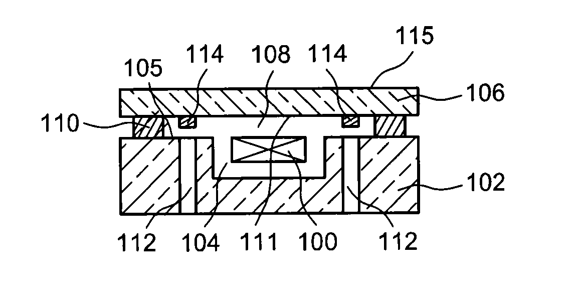
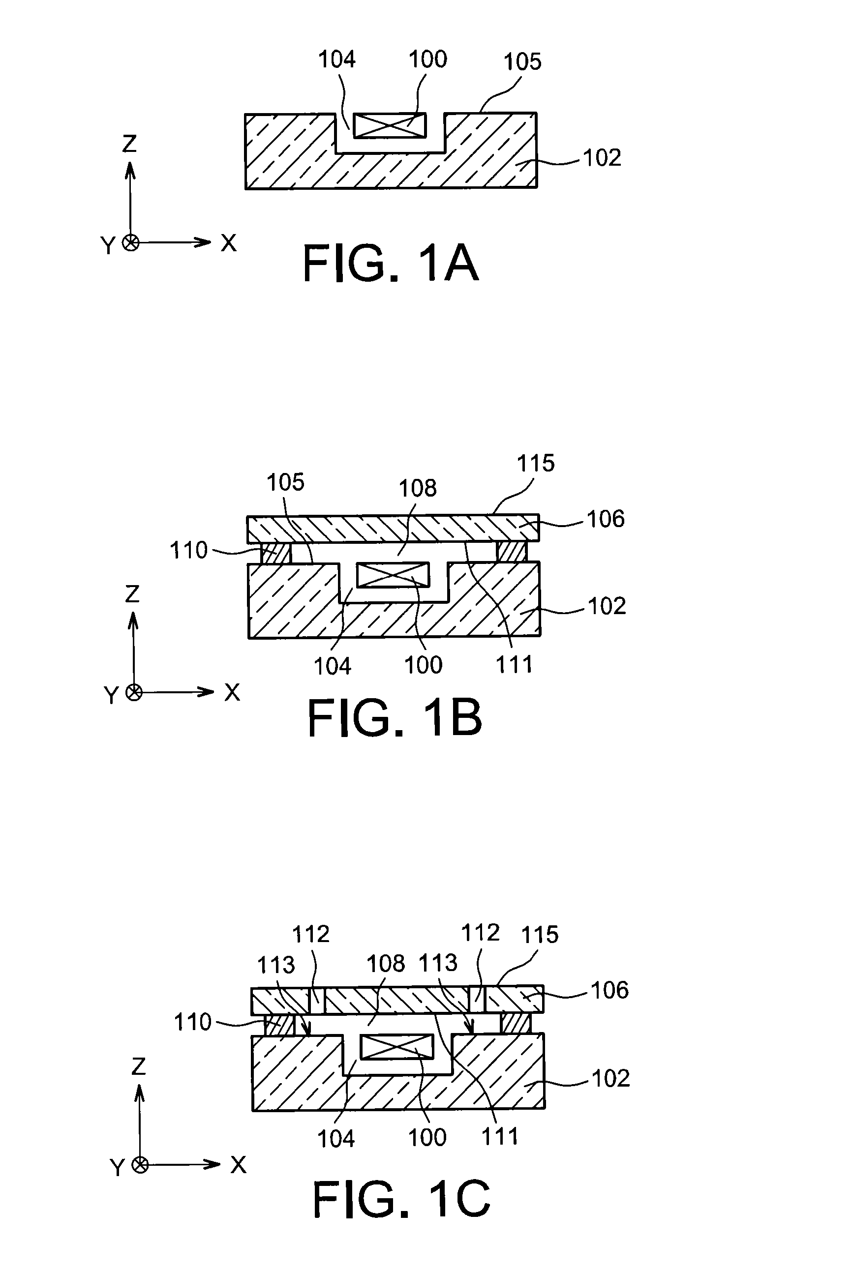
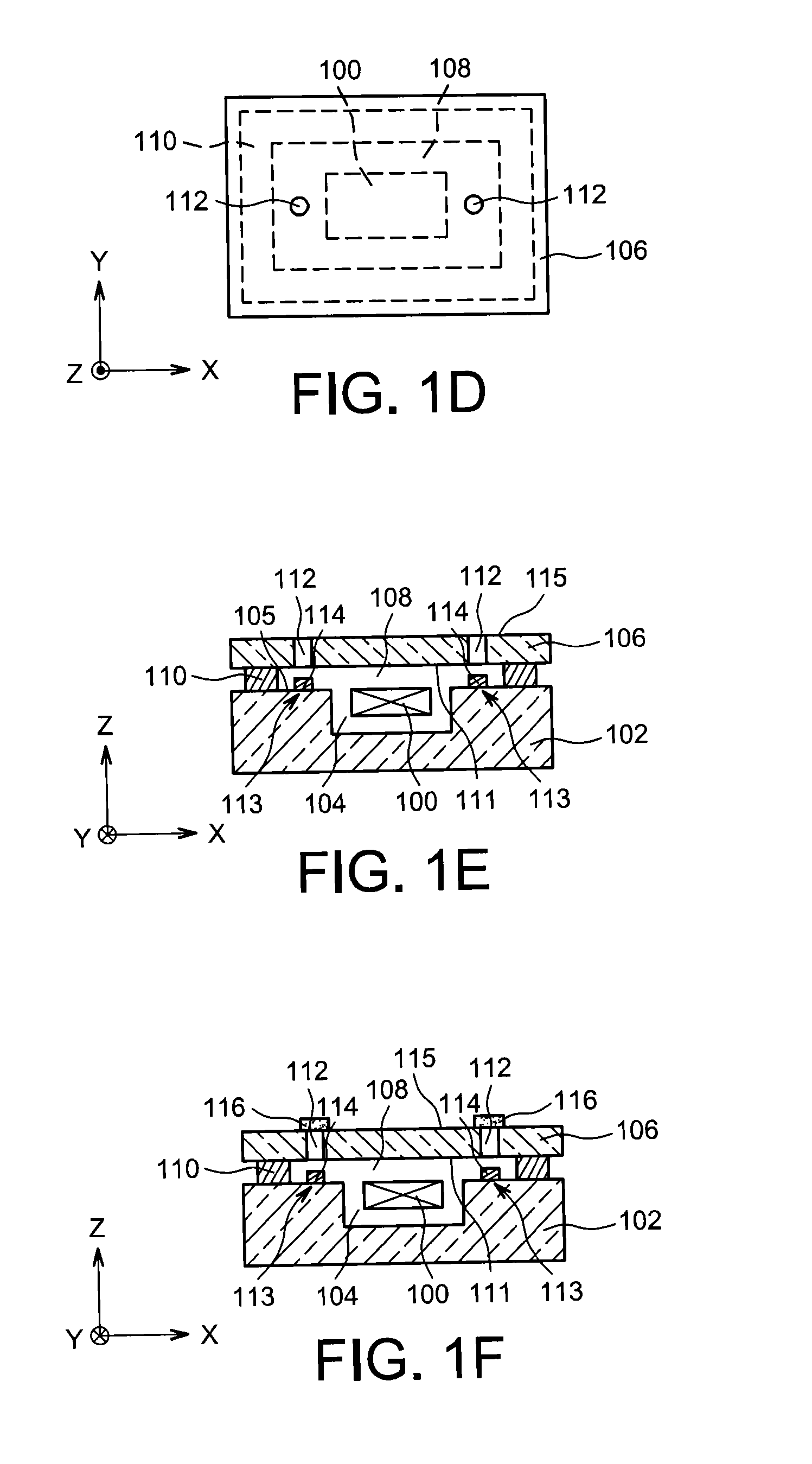
[0017]For this, one embodiment proposes a process for encapsulating a micro-device in a cavity formed between at least one first and one second substrate, comprising at least the steps of:[0018]producing the micro-device in and / or on the first substrate,[0019]attaching and securing the second substrate to the first substrate, forming the cavity in which the micro-device is placed,[0020]producing at least one hole through one of the two substrates, called the drilled substrate, and leading into the cavity opposite a portion of the other of the two substrates, called the receiving substrate,[0021]depositing at least one getter material portion on said receiving substrate portion through the hole,[0022]hermetically sealing the cavity by closing the hole.

[0023]Thus, the hole(s) may be produced throu...


PUM


Abstract

Process for encapsulating a micro-device in a cavity formed between one first and one second substrate, comprising at least the steps of:
    • producing the micro-device in and/or on the first substrate,
    • attaching and securing the second substrate to the first substrate, forming the cavity in which the micro-device is placed,
    • producing at least one hole through one of the two substrates, called the drilled substrate, and leading into the cavity opposite a portion of the other of the two substrates, called the receiving substrate,
    • depositing at least one getter material portion on said portion of the receiving substrate through the hole,
    • hermetically sealing the cavity by closing the hole.

Description

TECHNICAL FIELD[0001]The invention relates to a process for encapsulating a micro-device, microsystem or micro-component, for example of the MEMS, NEMS or MOEMS type or an infrared microsensor such as a microbolometer, in a hermetic cavity formed between two substrates and in which a getter material is deposited.PRIOR ART[0002]Some micro-devices such as those of the MEMS or NEMS type or infrared microsensors must, for successful operation, be hermetically sealed or encapsulated in a cavity of which the atmosphere is controlled (control in particular of the nature of the gas and pressure in the cavity).[0003]The technology used to obtain such an encapsulation consists first of producing these micro-devices collectively on a first silicon substrate (or wafer). Each of the micro-devices is then encapsulated in a cavity formed by attaching and hermetically sealing a cap, for example, formed by a second silicon substrate, on the first substrate. This hermetic assembly between the first a...

Claims


Application Information

Patent Timeline
IPC IPC(8): H01L21/56
CPCB81C1/00285H01L23/26B81C2201/019B81C2203/0118B81C2203/0145H01L2924/0002H01L21/50H01L2924/00
Inventor BAILLIN, XAVIERPORNIN, JEAN-LOUIS
Owner COMMISSARIAT A LENERGIE ATOMIQUE ET AUX ENERGIES ALTERNATIVES
Why Eureka
Try Eureka