Bond pad structure and fabricating method thereof

a bond pad and fabrication method technology, applied in semiconductor devices, semiconductor/solid-state device details, electrical devices, etc., can solve the problems of bond pad damage, material peeling, and undercutting of the sidewall of the opening, so as to avoid the damage of the bond pad structure, prevent undercutting, and improve the etching resistance

Active Publication Date: 2013-04-18
MARLIN SEMICON LTD
View PDF4 Cites 24 Cited by
  • Summary
  • Abstract
  • Description
  • Claims
  • Application Information

AI Technical Summary

Benefits of technology

[0022]Because, the isolation layer has better etching resistance in comparison with the ILD layer of the interconnection structure, when the sidewalls of the opening are thoroughly covered by the isolation layer, it is more likely to prevent undercuts occurring in the interconnection structure and avoid the bond pad structure from being damaged due to the impacts of the subsequent manufacturing procedurals. Besides, since facilitating the bond pad structure can reduce the use of reticles in the subsequent manufacturing procedurals, thus the fabrication process can be simplified, the manufacturing cost should be significantly reduced and the objects of the present invention can be reached.

Problems solved by technology

Because both of the MEMS devices and the bond pads of these micro-electromechanical elements generally need to be exposed form the wafer surface via an opening, thus undercuts may occur on the sidewalls of the openings used to expose the bond pad of these micro-electromechanical elements due to the etching process subsequently performed to form the openings for exposing the MEMS devices.
Accordingly, the bond pads may be damage by the impact of the die sawing process or the subsequent manufacturing procedurals, and at the worst case, material peeling may even occur.
Therefore, how to avoid the bond pad structure from damage due to the impacts of the subsequent manufacturing procedurals is still a challenge to the art.

Method used


Image

  • Bond pad structure and fabricating method thereof
  • Bond pad structure and fabricating method thereof
  • Bond pad structure and fabricating method thereof

Examples


Embodiment Construction

[0027]Detail descriptions of several embodiments eligible to exemplify the features of making and using the present invention are disclosed as follows. It must be appreciated that the following embodiments are just exemplary, but not being used to limit the scope of the present invention. Wherever possible, the same reference numbers are used in the drawings and the description to refer to the same or like parts.

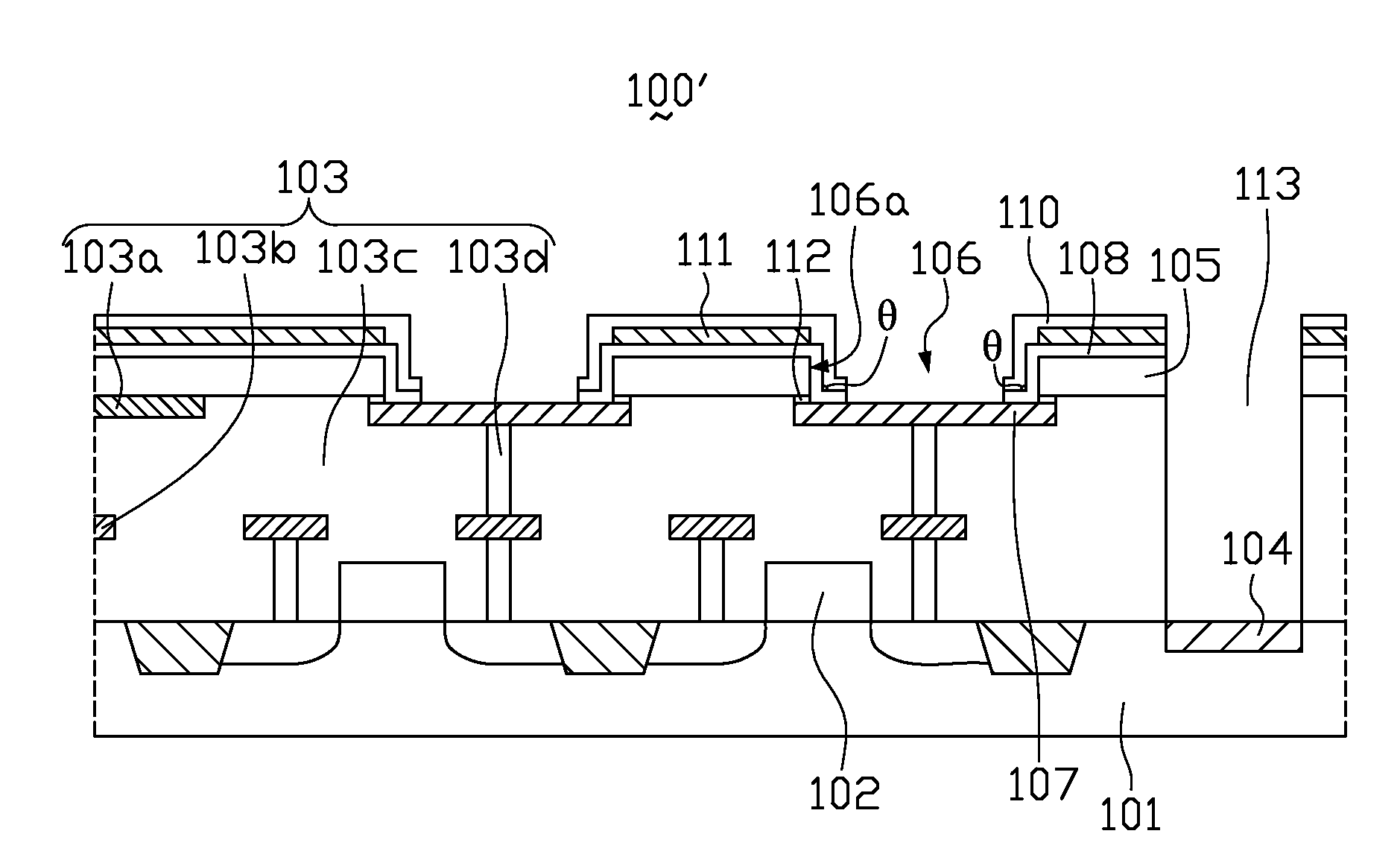
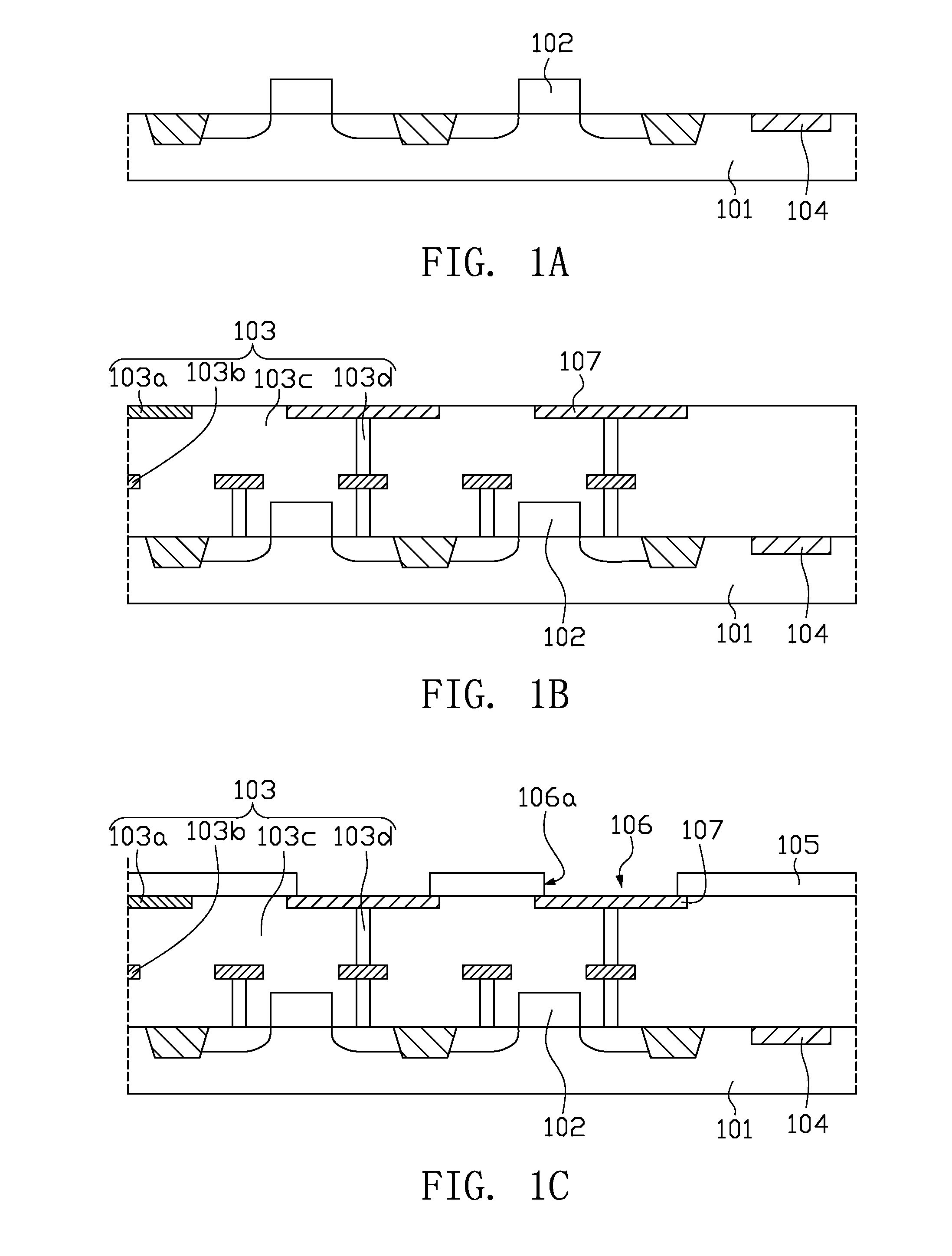
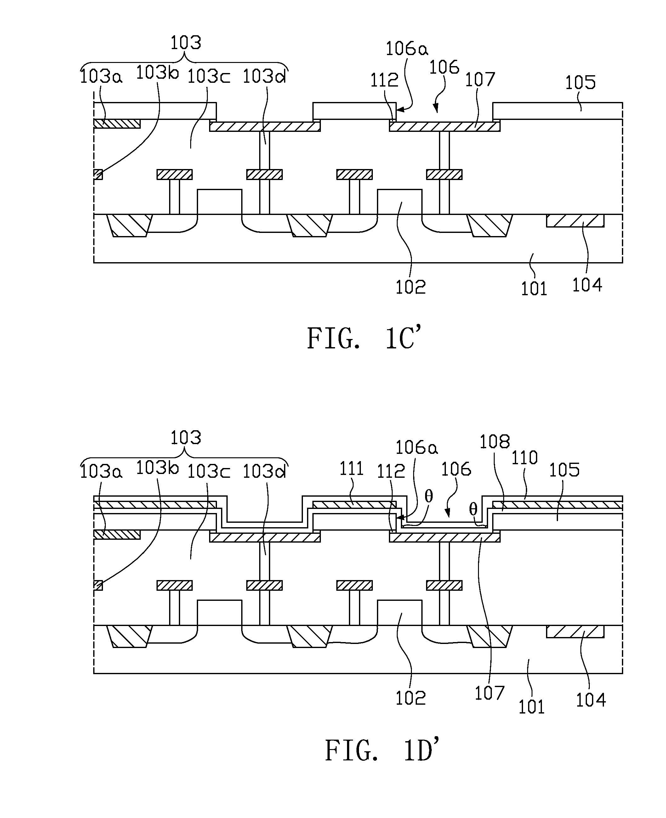
[0028]FIGS. 1A to 1E are cross sectional views illustrating the process for manufacturing a MEMS device 100, in accordance with one embodiment of the present invention. In some embodiments of the present invention, the MEMS device 100 may be a micro-acoustical sensor, a gyro-sensor, an accelerometer or a clock generation and oscillator.

[0029]The process for fabricating the MEMS device 100 comprises steps as follows: Firstly, a substrate 101 having at least one micro-electromechanical element 104 and an electrical device used for receiving, dealing with or transmitting signal...


PUM


Abstract

A bond pad structure comprises an interconnection structure and an isolation layer. The dielectric layer has an opening and a metal pad. The isolation layer is disposed on the interconnection structure and extends into the opening until it is in contact with the metal pad, whereby the sidewalls of the opening is blanketed by the isolation layer, and a portion of the metal pad is exposed from the opening.

Description

BACKGROUND OF THE INVENTION[0001]1. Field of Invention[0002]The present invention relates to a semiconductor device and the fabricating method thereof and more particularly relates to a bond pad structure and the fabricating method thereof.[0003]2. Description of Related Art[0004]Along with the improvement of the electrical technology, providing consumers a consumer electronic product with smaller size and more functions is continuously required. To satisfy the requirement, micro-electro-mechanical systems (MEMS) device, such as a micro-acoustical sensor, a gyro-sensor, an accelerometer or a clock generation and oscillator are consequently involved in the consumer electronic products.[0005]A typical MEMS device is formed by a semiconductor process, wherein a plurality of micro-electromechanical elements are directly minimized and formed on a wafer, so as to be integrated with a circuit used for receiving, treating or transmitting signals resulted form the micro-electromechanical ele...

Claims


Application Information

Patent Timeline
Patent Type & Authority Applications(United States)
IPC IPC(8): H01L23/485H01L21/768
CPCH01L24/00H01L2924/1461H01L2924/00B81B7/0006B81B2207/015H01L23/291H01L23/293H01L23/3192H01L24/05H01L2224/0401H01L2224/04042H01L2224/04073H01L2224/05567H01L2224/05624H01L2924/00014
Inventor WU, HUI-MINWANG, MING-IWANG, KUAN-YUHSIEH, KUN-CHEHUANG, CHIEN-HSIN
Owner MARLIN SEMICON LTD
Why Eureka
Try Eureka