Multilayer photoresist systems

a technology of resist thickness and diffusion step, applied in the field of multi-layer photoresist systems, can solve the problems of increasing resist thickness over diffusion step on substrate, affecting the focus of exposure tools, step and scan tools,

Active Publication Date: 2009-09-01
ROHM & HAAS ELECTRONICS MATERIALS LLC
View PDF59 Cites 23 Cited by
  • Summary
  • Abstract
  • Description
  • Claims
  • Application Information

AI Technical Summary

Benefits of technology

[0022]Suitable underlayer compositions also may be substantially free of a separate crosslinker component and / or an acid or acid generator compound. Such compositions will be preferably thermally treated under relatively vigorous conditions to effect hardening / crosslinking, e.g. at least 180° C., 190° C. or 200° C. for a time sufficient for hardening such as 0.5, 1 or 2 minutes.

Problems solved by technology

However, at shorter wavelengths the depth of focus of the exposure tool, which may be an excimer stepper, or step and scan tool, may be adversely affected.
However, the major drawback of using a thin layer of resist is that the variation of resist thickness over a diffusion step on a substrate and into an etched pattern increases as the pattern size becomes smaller.
Therefore, in a single layer resist system, the lack of dimensional control on the wafer can create different line widths throughout the resist which reduces the quality of the electronic package.

Method used


Image

  • Multilayer photoresist systems
  • Multilayer photoresist systems
  • Multilayer photoresist systems

Examples


example 1

Underlayer Composition of the Invention

[0096]An underlayer (bottom layer) composition of the invention is prepared by admixing the following materials in the specified amounts:

Resins

[0097]Poly(vinylphenol) having mesyl substitution

[0098]Terpolymer containing polymerized units of methylmethylacrylate / anthracene acrylate / ethylhydroxyacrylate

Crosslinkers

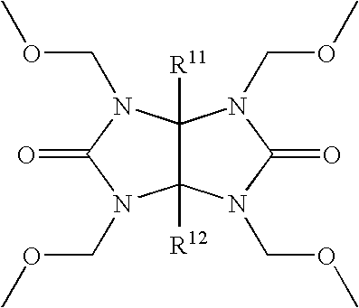
[0099]3-methyl-6-propyl-tetramethoxy glycoluril (in an amount of 4.5 weight % of resin component)

[0100]hexamethoxymethyl melamine (tradename Cymel) (in an amount of 5 weight % of resin component)

Acid Generator

[0101]Dodecylbenzene sulfonic acid (tradename Nacure 5225) (in an amount of 0.5 weight % of resin component)

Surfactant

[0102]Siloxane surfactant (in an amount of 0.3 weight % of resin component)

Solvent

[0103]90:10 v:v blend of propylene glycol monomethyl ether:ethyl lactate (to provide 90 weight % fluid formulation)

example 2

Photoresist Preparation

[0104]Part A. Silicon-containing Polymer Preparation.

[0105]Part 1.

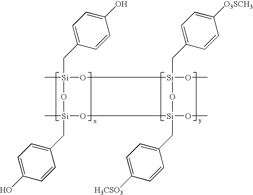
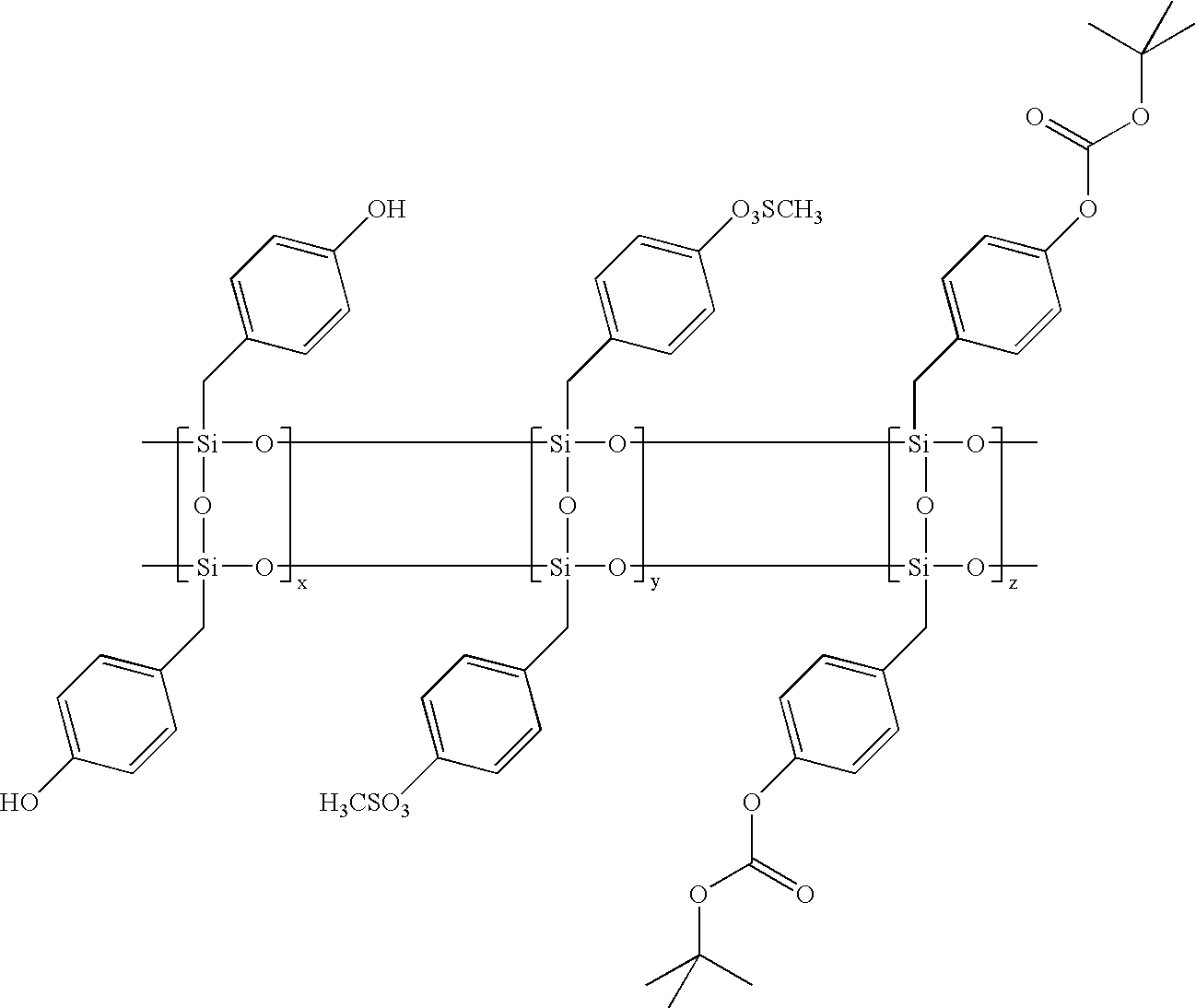
[0106]Poly(4-hydroxybenzyl silsesquioxane) (254.7 g) is dissolved in 1000 mL dry acetone under nitrogen atmosphere in a dried 3 L flask (reactor). Methanesulfonyl chloride (23.8 g) is added and the reactor is cooled to 15° C. A solution of distilled triethylamine (21.9 g) and acetone (22 g) is gradually added dropwise over 20-30 minutes, maintaining a reaction temperature of less than 30° C. Stirring is continued for 3 hours, at which time the solution is added dropwise over 2 h. to 32 L of water, precipitating the polymer. The polymer is then collected by suction filtration, and suspended in 8 L of water with stirring at room temperature for 18 h. The solid is then collected by suction filtration, is washed with water until the effluent is pH neutral, air-dried for 48 h., and is then dried in vacuo for 24 h. at 70° C. to yield an off-white polymer, having the formula 95 mol % hydroxybenzylsilse...

example 3

Multilayer Photoresist System

[0113]The underlayer composition prepared in Example 1 above is spin-coated onto an 8 inch silicon wafer and baked at 175° C. for 60 seconds to remove solvent and provide a crosslinked coating layer.

[0114]A silicon-containing photoresist of Example 2 above is applied over the thus thermally treated underlayer by spin-coating. This sample is spin coated on a wafer, is baked at 90° C. for 90 seconds, and is then imaged on an ASML 0.63 NA DUV stepper using a Global 5-Line reticle and annular illumination (0.85 outer, 0.55 inner).


PUM

PropertyMeasurementUnit
wavelengthaaaaaaaaaa
wavelengthsaaaaaaaaaa
thicknessaaaaaaaaaa

Abstract

Multilayer photoresist systems are provided. In particular aspects, the invention relates to underlayer composition for an overcoated photoresist, particularly an overcoated silicon-containing photoresist. Preferred underlayer compositions comprise one or more resins or other components that impart etch-resistant and antireflective properties, such as one or more resins that contain phenyl or other etch-resistant groups and anthracene or other moieties that are effective anti-reflective chromophores for photoresist exposure radiation.

Description

[0001]This application claims the benefit of U.S. Provisional Application No. 60 / 427,809 filing date Nov. 20, 2002BACKGROUND[0002]1. Field of the Invention[0003]The present invention relates generally to multilayer photoresist systems. In particular aspects, the invention relates to underlayer compositions for use with an overcoated photoresist, particularly an overcoated silicon-containing photoresist.[0004]2. Background[0005]Photoresists are photosensitive films used for transfer of images to a substrate. A coating layer of a photoresist is formed on a substrate and the photoresist layer is then exposed through a photomask to a source of activating radiation. The photomask has areas that are opaque to activating radiation and other areas that are transparent to activating radiation. Exposure to activating radiation provides a photoinduced chemical transformation of the photoresist coating to thereby transfer the pattern of the photomask to the photoresist-coated substrate. Followi...

Claims


Application Information

Patent Timeline
Patent Type & Authority Patents(United States)
IPC IPC(8): G03F7/00G03F7/004G03F7/11G03F7/075G03F7/09H01L21/027
CPCG03F7/0755G03F7/0757G03F7/0758G03F7/094G03F7/091Y10S430/128Y10S430/106G03F7/075
Inventor CAMERON, JAMES F.GRONBECK, DANA A.BARCLAY, GEORGE G.
Owner ROHM & HAAS ELECTRONICS MATERIALS LLC
Why Eureka
Try Eureka