Contact terminal for a probe card, and the probe card

a technology of contact terminal and probe card, which is applied in the direction of semiconductor/solid-state device testing/measurement, instruments, measurement devices, etc., can solve the problems of contact terminal being damaged by melting and the resistance of contact terminal increasing, so as to reduce the conductance of electric current, high resistivity, and high abrasion resistance materials

Inactive Publication Date: 2013-04-25
TOKYO ELECTRON LTD
View PDF0 Cites 26 Cited by
  • Summary
  • Abstract
  • Description
  • Claims
  • Application Information

AI Technical Summary

Benefits of technology

[0006]However, high abrasion resistant materials generally have a high resistivity, and the contact terminal has reduced electric current conductance due to its smaller size, and thus, the resistance of the contact terminal increases. Thus, when an electric current is applied to the contact terminal, the contact terminal emits a heat not only to be oxidized but to oxidize surrounding contact terminals. In addition, when the amount of heat emitted by the contact terminal is remarkable, the contact terminal may be damaged by melting.

Problems solved by technology

However, high abrasion resistant materials generally have a high resistivity, and the contact terminal has reduced electric current conductance due to its smaller size, and thus, the resistance of the contact terminal increases.
In addition, when the amount of heat emitted by the contact terminal is remarkable, the contact terminal may be damaged by melting.

Method used


Image

  • Contact terminal for a probe card, and the probe card
  • Contact terminal for a probe card, and the probe card
  • Contact terminal for a probe card, and the probe card

Examples


Embodiment Construction

[0023]Hereinafter, embodiments of the present invention will be described with reference to the accompanying drawings which form a part hereof.

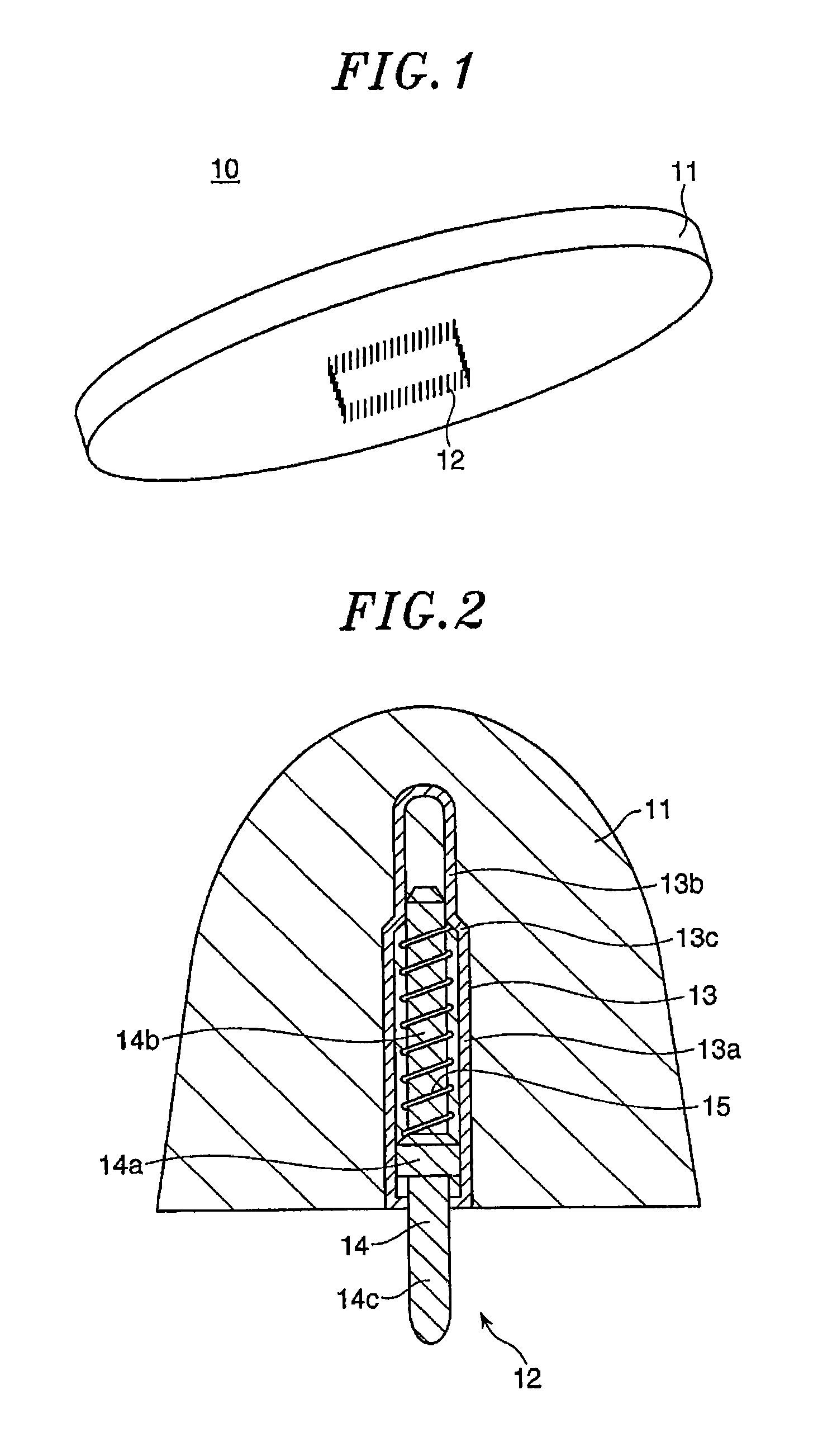
[0024]FIG. 1 is a perspective view schematically illustrating a configuration of a probe card in accordance with the embodiment of the present invention.

[0025]Referring to FIG. 1, the probe card 10 includes a circular plate-shaped base 11 (base portion) and pogo pins 12 disposed on a surface of the base 11 facing a semiconductor wafer (the bottom surface in FIG. 1).

[0026]The pogo pins 12 are disposed corresponding to electrode pads or solder bumps arranged on a semiconductor device formed on the semiconductor wafer, and thus, tips thereof can be brought in contact with the respective electrode pads or solder bumps when the probe card 10 faces the semiconductor wafer.

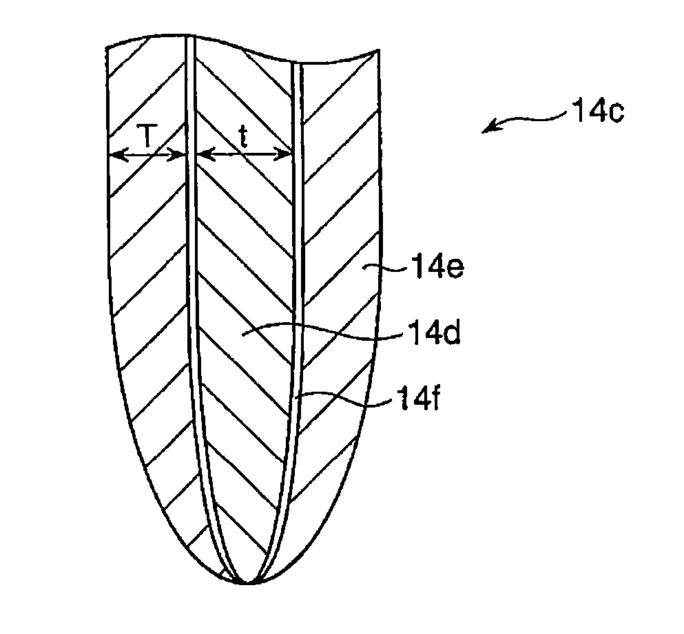
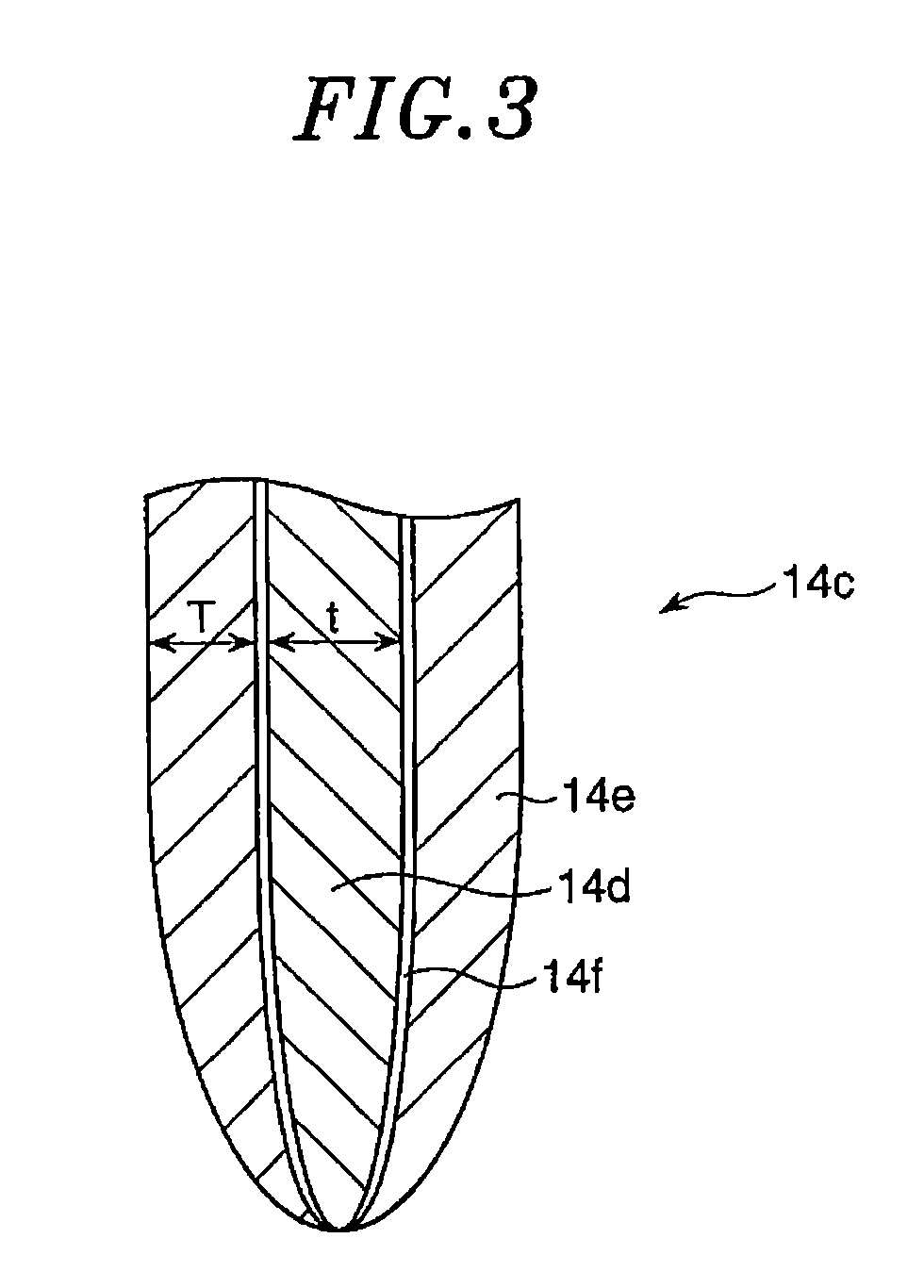
[0027]FIG. 2 is an enlarged cross-sectional view schematically illustrating a configuration of the pogo pin 12 shown FIG. 1.

[0028]Referring to FIG. 2, the pogo pin 12 includes a t...


PUM

PropertyMeasurementUnit
thicknessaaaaaaaaaa
thicknessaaaaaaaaaa
thicknessaaaaaaaaaa

Abstract

A contact terminal for a probe card includes a cylindrical main body. The main body includes a pillar-shaped central portion formed of a first material and an outer housing which is formed of a second material and covers a lateral surface of the central portion, and hardness and resistivity of the second material are different from hardness and resistivity of the first material. The hardness of the second material is higher than that of the first material and the resistivity of the first material is lower than that of the second material, or the hardness of the first material is higher than that of the second material and the resistivity of the second material is lower than that of the first material.

Description

CROSS-REFERENCE TO RELATED APPLICATION[0001]This application claims priority to Japanese Patent Application No. 2011-231673 filed on Oct. 21, 2011, the entire contents of which are incorporated herein by reference.FIELD OF THE INVENTION[0002]The present invention relates to a contact terminal for a probe card and the probe card.BACKGROUND OF THE INVENTION[0003]A probe is used as a detecting unit to examine each semiconductor device formed on a wafer. The probe includes a stage on which a wafer is mounted and a probe card to face the stage. The probe card includes a plate-shaped base and cylindrical contact terminals, such as plungers or contact probes of pogo pins (spring probes), disposed on a surface of the base facing the stage to face electrode pads or solder bumps of the semiconductor device of the wafer (e.g., see Japanese Application Publication No. 2002-22768).[0004]In the probe, when the wafer mounted on the stage faces the probe card, the respective contact terminals of th...

Claims


Application Information

Patent Timeline
Patent Type & Authority Applications(United States)
IPC IPC(8): G01R1/067G01R31/26
CPCG01R1/06755G01R1/06722G01R1/06738G01R1/073H01L22/00
Inventor HOSHINO, TOMOHISAAMEMIYA, TAKASHI
Owner TOKYO ELECTRON LTD
Why Eureka
Try Eureka