

3-d nonvolatile memory device and method of manufacturing the same, and memory system including the 3-d nonvolatile memory device
a nonvolatile memory and non-volatile technology, applied in the field of non-volatile memory devices, can solve the problems of difficult to ensure operation reliability and damage to the gate insulating layer of select transistors, and achieve the effect of improving reliability
- Summary
- Abstract
- Description
- Claims
- Application Information
AI Technical Summary
Benefits of technology
Problems solved by technology
Method used
Image

Examples
first embodiment
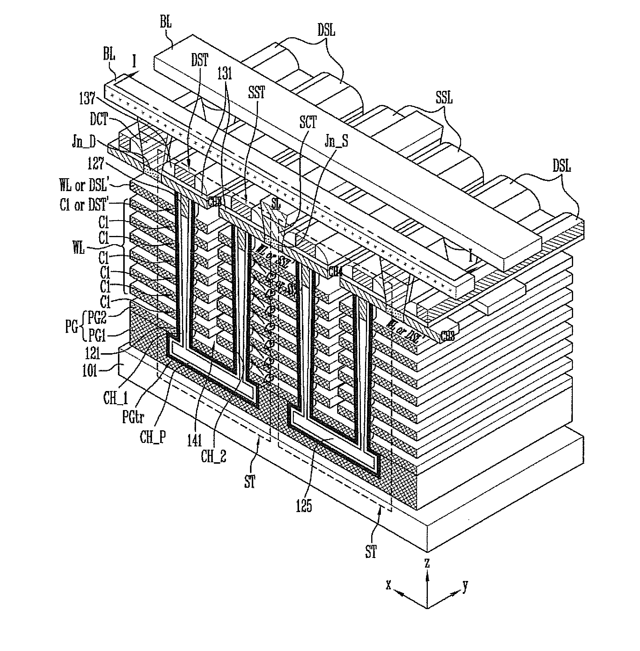
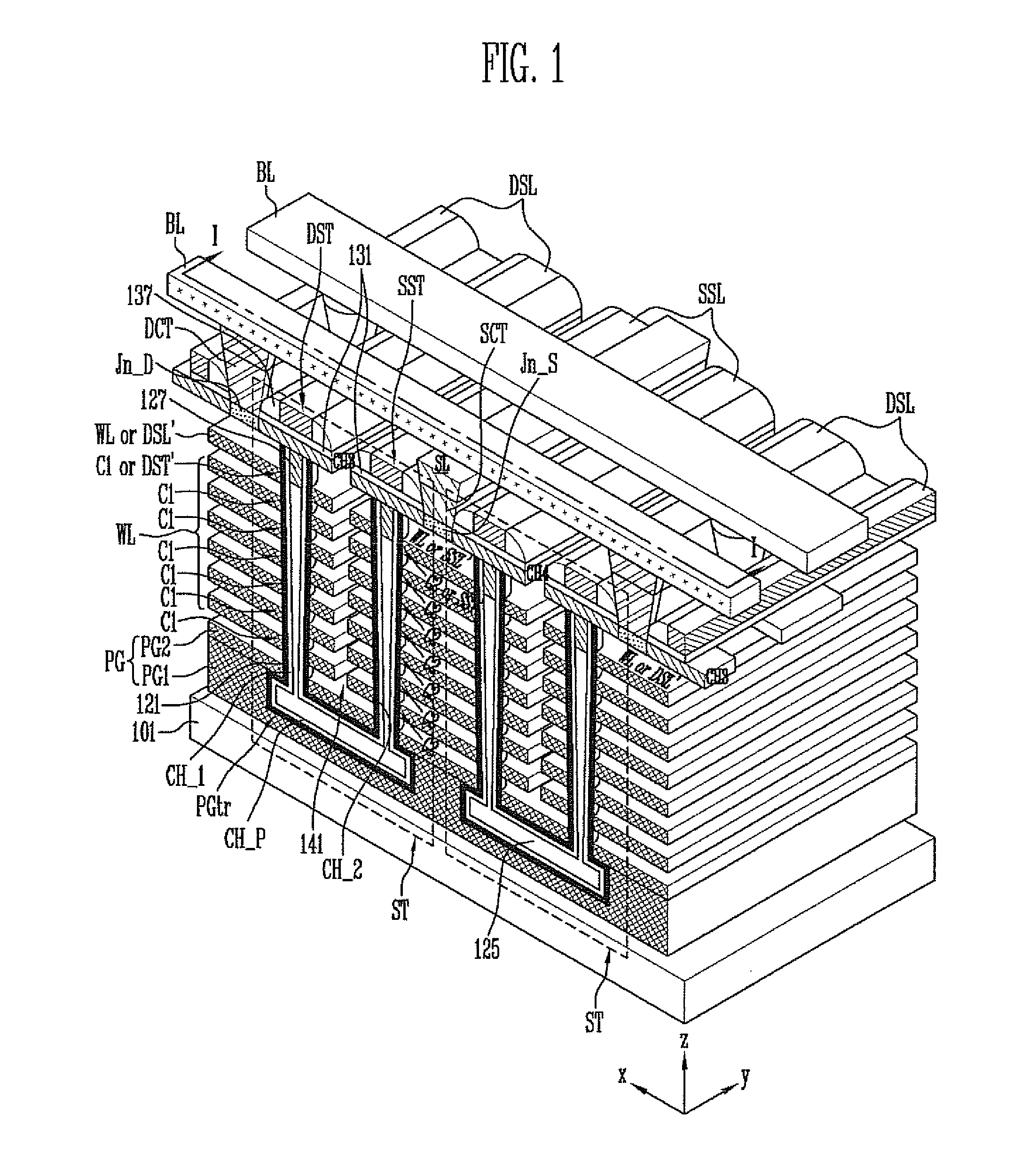
[0023]FIG. 1 is a perspective view of a 3-D nonvolatile memory device according to this disclosure. In FIG. 1, interlayer insulating layers and gap-fill insulating layers formed within slits 141 are not shown, for simplicity.
[0024]Referring to FIG. 1, the 3-D nonvolatile memory device according to the first embodiment include bit lines BL, a source line SL formed to cross the bit lines BL and isolated from the bit lines BL, and a memory string ST coupled between the source line SL and the bit line BL. Some memory strings ST arranged in a direction where the bit lines BL are extended are coupled in parallel to the respective bit lines BL. Some memory strings ST arranged in a direction where the source line SL is extended are coupled to the source line SL in common.
[0025]The bit lines BL are conductive patterns isolated from a substrate 101 and disposed over the substrate 101. The bit lines BL are isolated from each other and disposed in parallel. For example, the bit lines BL may be ...
second embodiment
[0085]FIG. 4 is a perspective view of a 3-D nonvolatile memory device according to this disclosure. In particular, the 3-D nonvolatile memory device of FIG. 4 has the same construction as the 3-D flash memory device of FIG. 1 except regions where slits are formed. Interlayer insulating layers and a gap-fill insulating layer formed within the slits are not shown in FIG. 4, for simplicity.
[0086]Like in FIG. 1, in FIG. 4, the nonvolatile memory device according to the second embodiment includes bit lines BL, a source line SL configured to cross the bit lines BL and isolated from the bit lines BL, and memory strings ST coupled between the source line SL and the bit lines BL. Unlike in the first embodiment of FIG. 1, in the second embodiment, a slit 241a is formed between the first vertical channel layers CH_1, between the second vertical channel layers CH_2 under the source and drain junctions Jn_S and Jn_D, between the first and the second planar channel layers CH_3 and CH_4, and betwe...
third embodiment
[0112]FIG. 6 is a cross-sectional view illustrating a 3-D nonvolatile memory device and a method of manufacturing the same according to this disclosure.
[0113]Referring to FIG. 6, the 3-D nonvolatile memory device according to the third embodiment includes a source region 303, a bit line BL, and a plurality of memory strings ST disposed between the source region 303 and the bit line BL.
[0114]The source region 303 is formed by implanting an impurity into a substrate 301 or a doped silicon layer formed over the substrate 301. A plurality of the memory strings ST forming a memory block may be coupled in common over the source region 303.
[0115]The bit line BL is a conductive pattern isolated from the substrate 301 and disposed over the substrate 301. The plurality of memory strings ST is coupled in parallel under the bit line BL.
[0116]Each of the memory strings ST includes memory cells C stacked along each of vertical channel layer 323 upwardly protruded from the substrate 301, a lower s...
PUM
 Abstract
Description
Claims
Application Information