Jig for use in semiconductor test and method of measuring breakdown voltage by using the jig

a technology of breakdown voltage and jig, which is applied in the direction of measuring devices, instruments, testing dielectric strength, etc., can solve the problems of inability to accurately measure breakdown voltage, power supply breakage of measuring system, and semiconductor chip breakage, and achieve the effect of low cos

Active Publication Date: 2013-05-02
MITSUBISHI ELECTRIC CORP
View PDF12 Cites 24 Cited by
  • Summary
  • Abstract
  • Description
  • Claims
  • Application Information

AI Technical Summary

Benefits of technology

[0010]It is an object of the present invention to provide a jig for use in a semiconductor test and a method of measuring a breakdown voltage by using the jig that are capable of measuring the breakdown voltage of a semiconductor chip at low cost without generating atmosphere discharge.
[0012]In the present invention, when a test object is placed on a stage and a jig base and a stage move in a direction in which they get closer to each other, a probe pin comes into contact with an electrode formed on the test object, and an insulating material comes into contact with both the test object and the stage. Thus, the breakdown voltage of a semiconductor chip can be measured at low cost without generating atmosphere discharge.

Problems solved by technology

This generates discharge in atmosphere (atmosphere discharge or creeping discharge), leading to a problem of breakage of the semiconductor chip and breakage of a power supply of the measuring system.
So, generation of atmosphere discharge makes it impossible to measure a breakdown voltage accurately.
As a result, even a semiconductor chip with inaccurate breakdown voltage characteristics cannot be evaluated (breakdown voltage thereof cannot be measured accurately) before the semiconductor chip is assembled into a package.
This leads to serious reduction in measurement efficiency.
As a result of shrinkage of the terminal structure, the insulation breakdown electric field of atmosphere extending from an opening edge of a protective film formed at a terminal portion to an edge portion of a chip is made smaller than insulation breakdown electric field in bulk, leading to a problem in that creeping discharge is generated easily.
There has also been a problem in that discharge easily damages a gate oxide film of a semiconductor device having an MOS (metal-oxide semiconductor) structure.
This entails costs so the electrical characteristics of a semiconductor chip cannot be measured at low cost.

Method used


Image

  • Jig for use in semiconductor test and method of measuring breakdown voltage by using the jig
  • Jig for use in semiconductor test and method of measuring breakdown voltage by using the jig
  • Jig for use in semiconductor test and method of measuring breakdown voltage by using the jig

Examples


first preferred embodiment

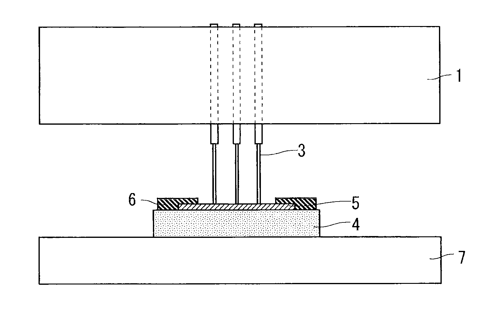
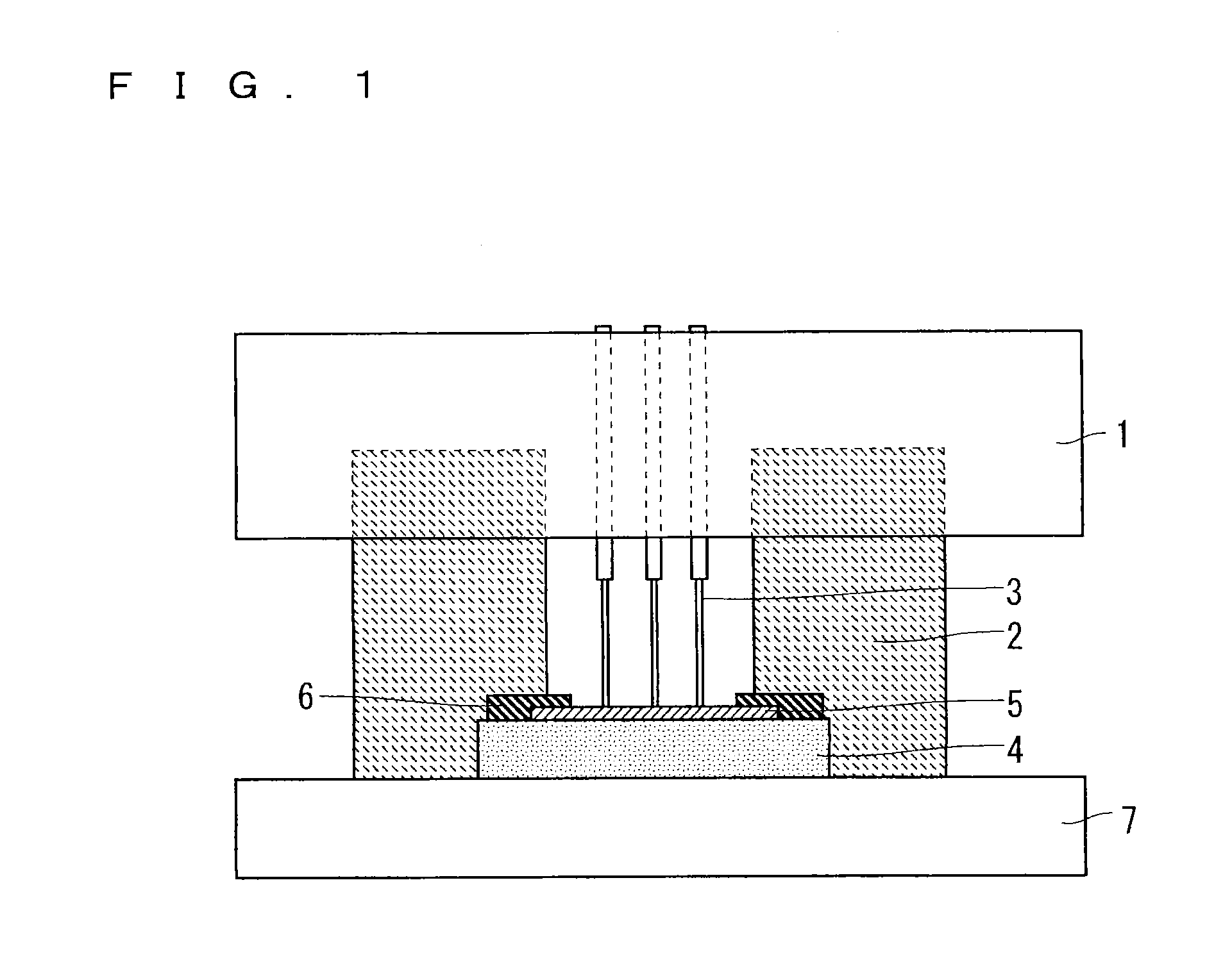
[0025]FIG. 1 shows an exemplary structure of a jig for use in a semiconductor test of a first preferred embodiment of the present invention. FIG. 1 shows a condition where measurement of a breakdown voltage (test) is performed by using the jig for use in a semiconductor test of the first preferred embodiment. As shown in FIG. 1, the jig for use in a semiconductor test of the first preferred embodiment includes a susceptor 1 (jig base) on which probe pins 3 and an insulating material 2 are provided such that the probe pins 3 are surrounded by the insulating material 2 having a hollow structure in plan view, and a lower electrode stage 7 (stage) arranged to face a surface of the susceptor 1 on which the probe pins 3 and the insulating material 2 are provided and which is capable of receiving a semiconductor chip 4 (test object) placed on a surface facing the susceptor 1. A surface electrode 5 is formed on a surface (surface facing the susceptor 1) of the semiconductor chip 4, and a pr...

second preferred embodiment

[0040]FIG. 4 shows an exemplary structure of a jig for use in a semiconductor test of a second preferred embodiment of the present invention. FIG. 4 shows a condition where a breakdown voltage is measured (test is conducted) by using the jig for use in a semiconductor test of the second preferred embodiment.

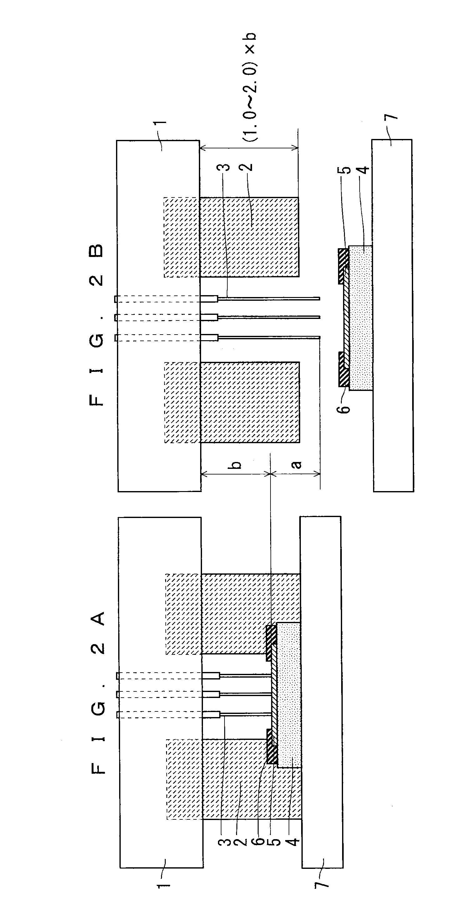
[0041]As shown in FIG. 4, in the jig for use in a semiconductor test of the second preferred embodiment, an insulating material 2 contacts a surface of a semiconductor chip 4 (test object) facing a susceptor 1 (jig base), at least part of a side surface of the semiconductor chip 4 continuous with this surface (in FIG. 4, upper part of the side surface), and a lower electrode stage 7 (stage). To be specific, in the jig for use in a semiconductor test of the second preferred embodiment, space is formed between the insulating material 2 and the side surface of the semiconductor chip 4 during a test. The structure and the operation of the jig for use in a semiconductor test of the se...

third preferred embodiment

[0043]FIGS. 5 and 6 each show an exemplary structure of a jig for use in a semiconductor test of a third preferred embodiment of the present invention. FIGS. 5 and 6 each show a condition where a breakdown voltage is measured (test is conducted) by using the jig for use in a semiconductor test of the third preferred embodiment.

[0044]As shown in FIG. 5, an insulating material 2 contacts a protective film 6, a side surface of a semiconductor chip 4, and a lower electrode stage 7. The insulating material 2 additionally contacts outer circumferential part of a surface electrode 5. Further, as shown in FIG. 6, probe pins 3 are surrounded by the insulating material 2 of a solid structure in plan view. To be specific, in the jig for use in a semiconductor test of the third preferred embodiment, the insulating material 2 additionally contacts the surface electrode 5 on the semiconductor chip 4 as shown in FIGS. 5 and 6. The structure and the operation of the jig for use in a semiconductor t...


PUM


Abstract

A jig for use in a semiconductor test of the present invention includes; a base on which a probe pin and an insulating material are provided such that the probe pin is surrounded by the insulating material in plan view; and a stage arranged to face a surface of the base on which the probe pin and the insulating material are provided. The stage is capable of receiving a test object placed on a surface facing the base. When the test object is placed on the stage and the base and the stage move in a direction in which they get closer to each other, the probe pin comes into contact with an electrode formed on the test object, and the insulating material comes into contact with both the test object and the stage.

Description

BACKGROUND OF THE INVENTION[0001]1. Field of the Invention[0002]The present invention relates to a jig for use in a semiconductor test and a method of measuring a breakdown voltage by using the jig. More specifically, the present invention relates to a jig for use in a semiconductor test and method of measuring a breakdown voltage by using the jig that are suitably applicable for measuring the breakdown voltage of a wide bandgap semiconductor.[0003]2. Description of the Background Art[0004]A power semiconductor device using a wide bandgap semiconductor being a semiconductor with a high breakdown voltage is subjected to measurement of electrical characteristics (hereinafter also called a test) when the power semiconductor device is in the form of a chip and has not been implemented on a package. Measurement items of electrical characteristics include measurement of a breakdown voltage. A breakdown voltage is considered as one of important indicators of performances, and should always...

Claims


Application Information

Patent Timeline
Patent Type & Authority Applications(United States)
IPC IPC(8): G01R31/26
CPCG01R1/07314G01R31/2623G01R31/261G01R31/129G01R19/00G01R31/12
Inventor IKEGAMI, MASAAKI
Owner MITSUBISHI ELECTRIC CORP
Why Eureka
Try Eureka