
Display panel

a display panel and panel technology, applied in the field of display panels, can solve the problems of gate driver not outputing a gate-on voltage at an appropriate time, reducing the spacing between transmission wires, and generating interference between the plurality of control signals, so as to increase the power consumption

Inactive Publication Date: 2013-05-02
SAMSUNG DISPLAY CO LTD
View PDF11 Cites 27 Cited by
  • Summary
  • Abstract
  • Description
  • Claims
  • Application Information

AI Technical Summary

Benefits of technology

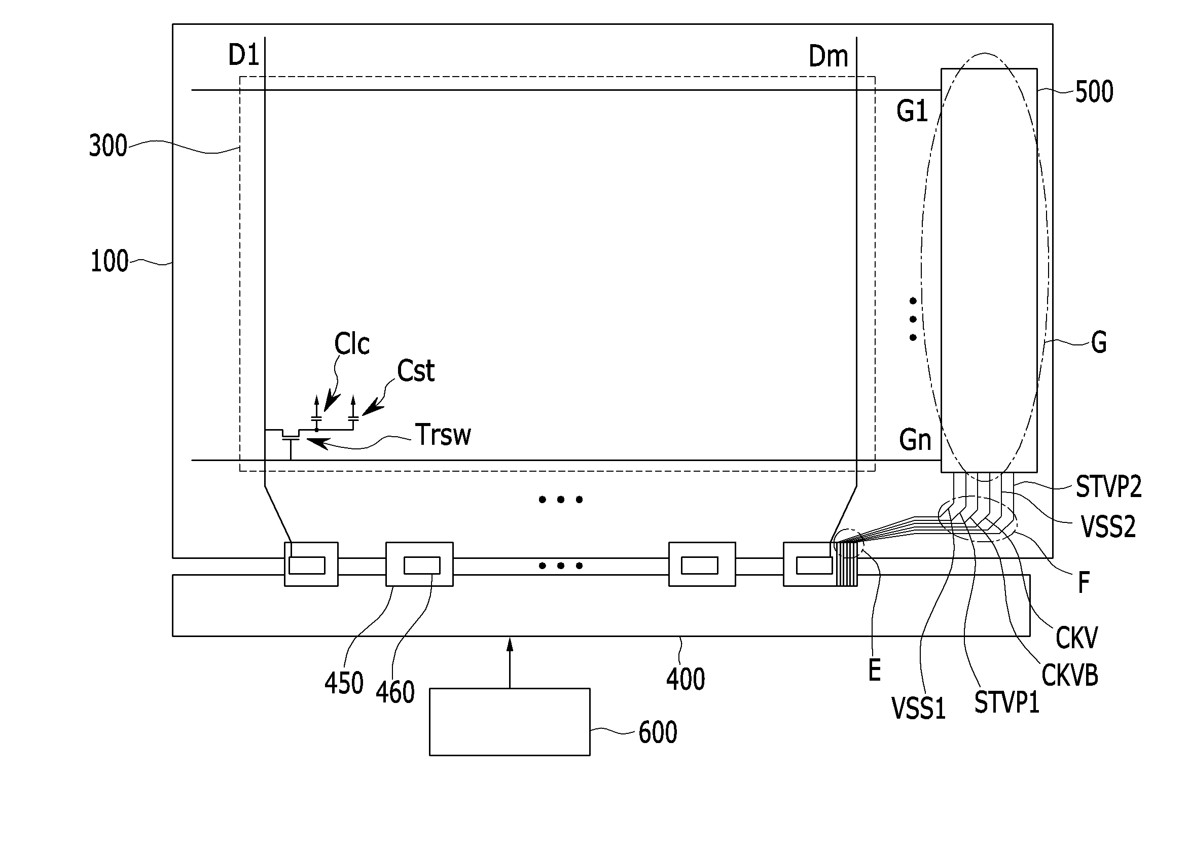
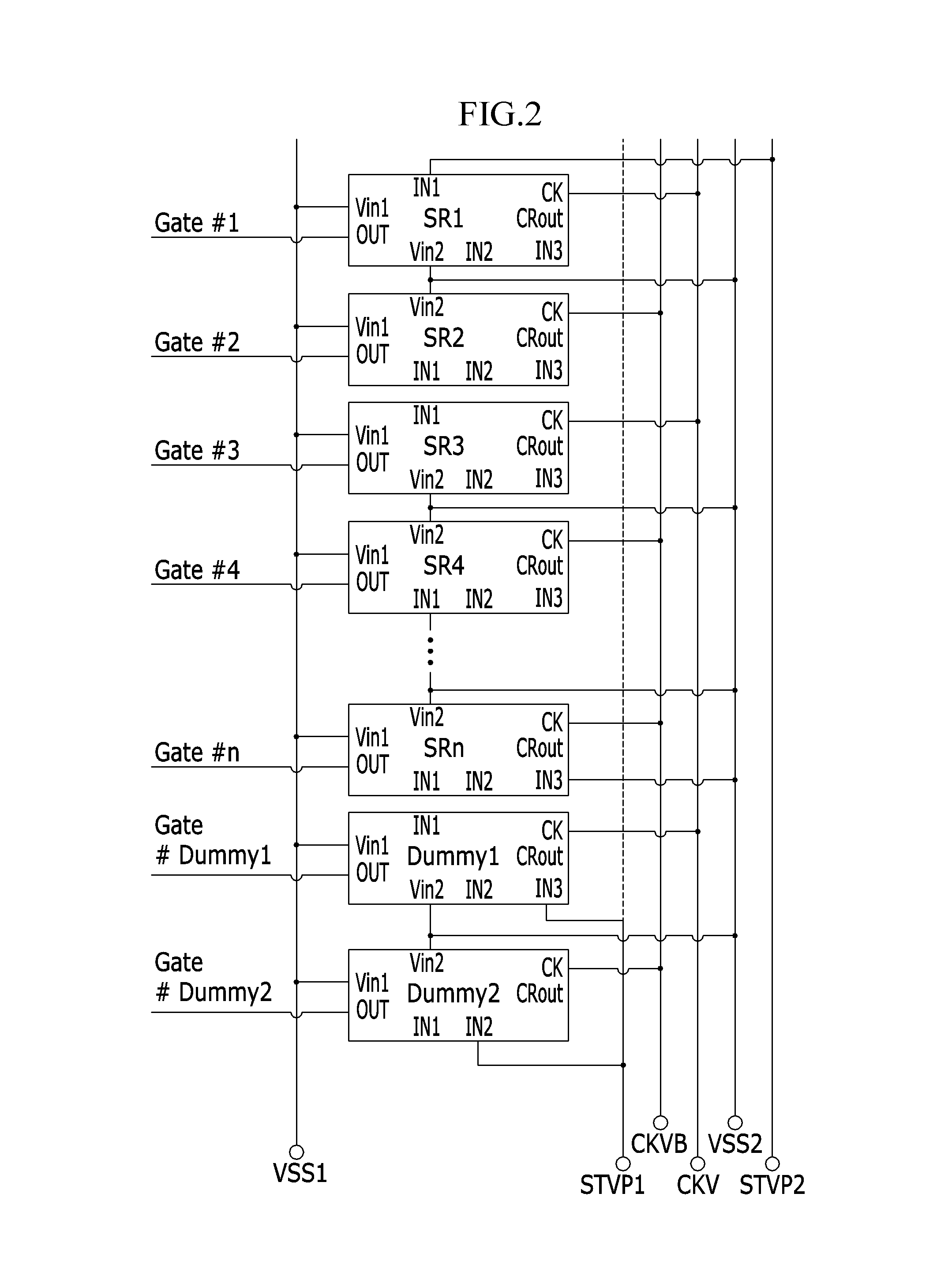
The invention reduces interference between control signals in a display panel to achieve a uniform waveform. This is achieved by dividing the wire supplying a scan start signal into two wires to avoid interference with the clock signal and other signals. This design prevents delays in the scan start signal and reduces power consumption by about 10% relative to designs that have overlapping wires.

Problems solved by technology

Such a reduced spacing between transmission wires may generate interference between the plurality of control signals.
If the timing of a control signal is delayed due to such interference, the gate driver may not output a gate-on voltage at an appropriate time.
As a result of the interference, horizontal stripes appear superimposed upon the image which mar the display quality.

Method used


Image

  • Display panel
  • Display panel
  • Display panel

Examples


Embodiment Construction

[0036]The present invention will be described more fully hereinafter with reference to the accompanying drawings, in which exemplary embodiments are shown. As those skilled in the art will realize, the described embodiments may be modified in various different ways, all without departing from the spirit or scope of the present invention.

[0037]In the drawings, the thickness of layers, films, panels, regions, etc., are exaggerated for clarity. Like reference numerals designate like elements throughout the specification. It will be understood that when an element such as a layer, film, region, or substrate is referred to as being “on” another element, it can be directly on the other element or intervening elements may also be present. In contrast, when an element is referred to as being “directly on” another element, there are no intervening elements present.

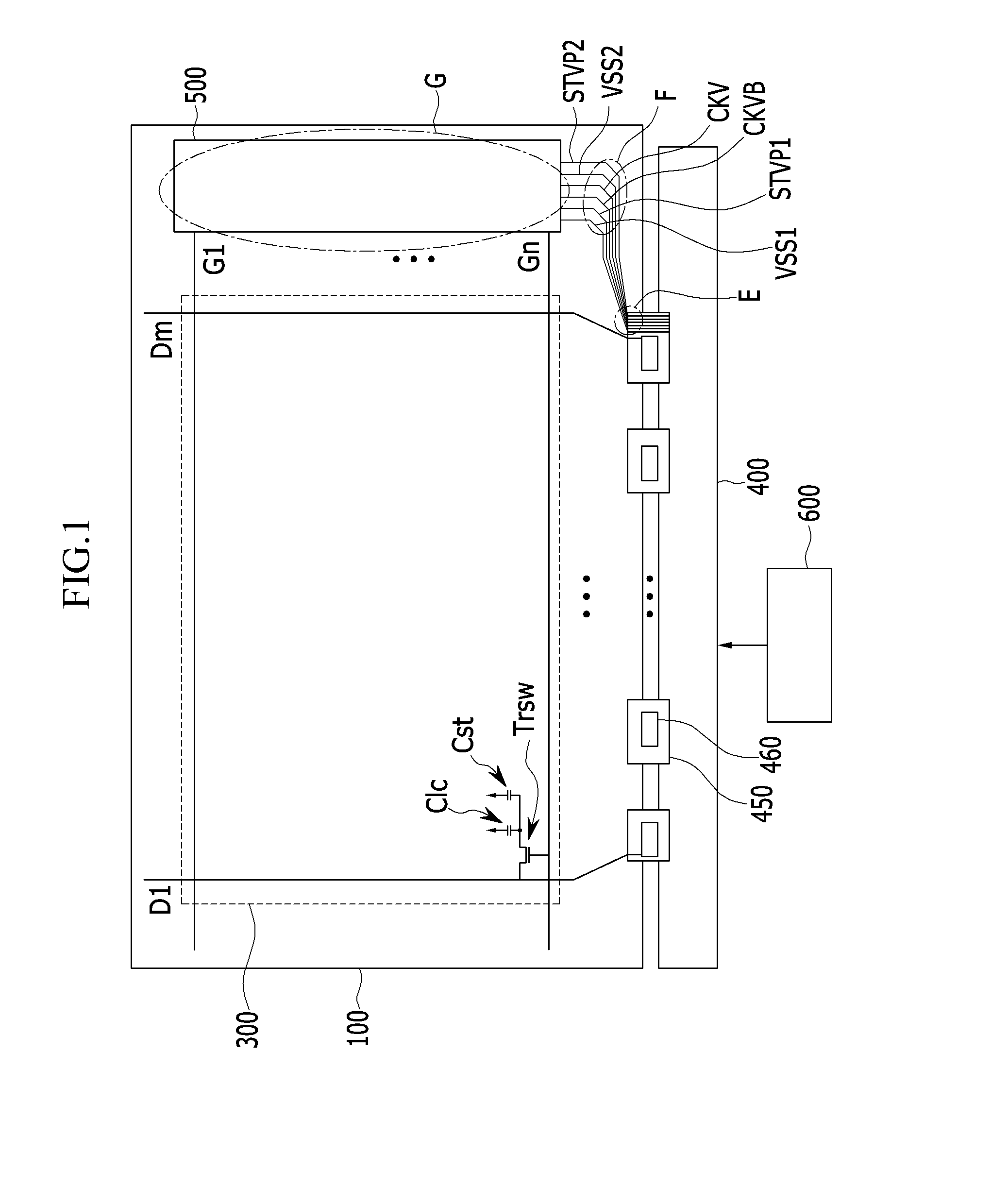
[0038]A display device will be described with reference to FIG. 1, a top plan view of a display panel according to an exemplary e...


PUM


Abstract

The present invention divides a wire supplying a scan start signal to a gate driver into two wires, so as to avoid overlapping a clock signal line. In this way the clock signal is not delayed by interference, and a gate driving margin may continue uninterrupted, thereby uniformly outputting a gate-on voltage. In particular, if the clock signal line is connected to all stages in the gate driver and the clock signal line overlaps the scan start signal line, unsightly horizontal bands appear on the image and the parallel gate lines generate a very large parasitic capacitance. In contrast, the gate drivers in the present disclosure comprise clock signal lines which do not overlap the scan start signal lines. As benefits, interference resulting in horizontal banding is minimized and the power consumption may be reduced by about 10%.

Description

CROSS-REFERENCE TO RELATED APPLICATION[0001]This application claims priority to and the benefit of Korean Patent Application No. 10-2011-0109850 filed in the Korean Intellectual Property Office on Oct. 26, 2011, the entire contents of which are incorporated herein by reference.BACKGROUND OF THE INVENTION[0002](a) Field of the Invention The present invention relates to a display panel, and preferably relates to a display panel having a gate driver integrated with a display panel.[0003](b) Description of the Related Art[0004]As a widely used flat panel display, the liquid crystal display (LCD) includes two glass panels, one provided with field generating electrodes such as pixel electrodes, and the other with a common electrode, and a liquid crystal layer interposed between the two panels. The LCD produces images by applying a potential to the field-generating electrodes, with the electric field re-orienting the LC molecules to change the transmission of incident polarized light. Othe...

Claims


Application Information

Patent Timeline
IPC IPC(8): G09G3/36
CPCG11C19/28G09G3/36G09G2320/0209G09G2310/0286G09G2310/0267
Inventor KOO, BON-YONGKIM, BEOM JUNKWON, HO KYOON
Owner SAMSUNG DISPLAY CO LTD
Learn More