Master-slave low-noise charge pump circuit and method

Active Publication Date: 2013-05-09
TEXAS INSTR INC
View PDF0 Cites 17 Cited by
  • Summary
  • Abstract
  • Description
  • Claims
  • Application Information

AI Technical Summary

Benefits of technology

[0009]It is an object of the invention to provide a low noise

Problems solved by technology

The reason for the large difference in frequency is due to the fact there is much higher voltage increase in the Dickson charge pumps than in the voltage triplers, and this causes a heavy current load on the voltage triplers that is sustained by operating the voltage triplers at a higher frequency tha

Method used


Image

  • Master-slave low-noise charge pump circuit and method
  • Master-slave low-noise charge pump circuit and method
  • Master-slave low-noise charge pump circuit and method

Examples


Example

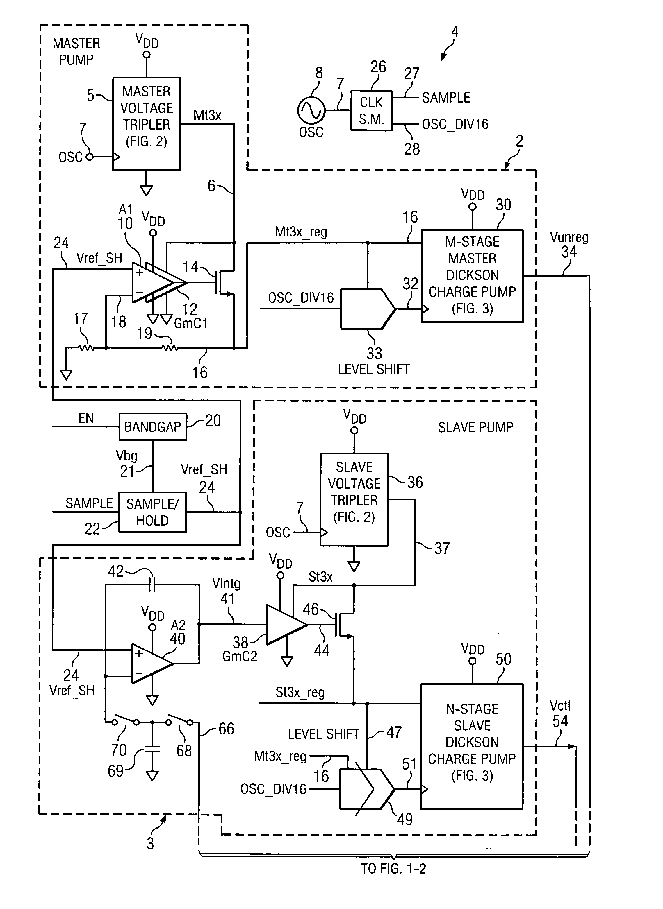
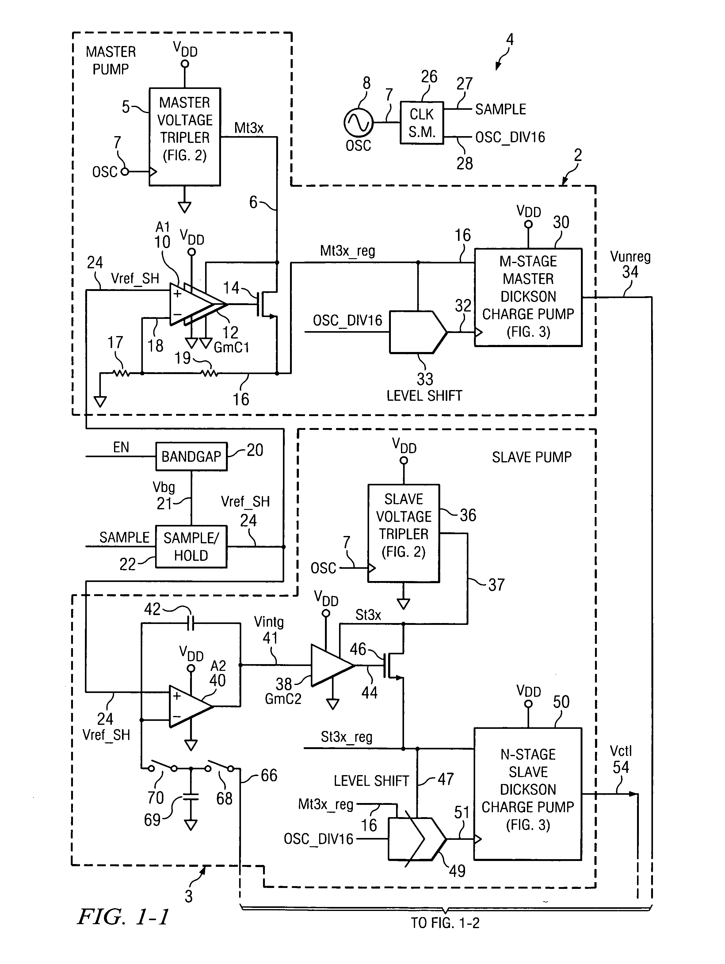
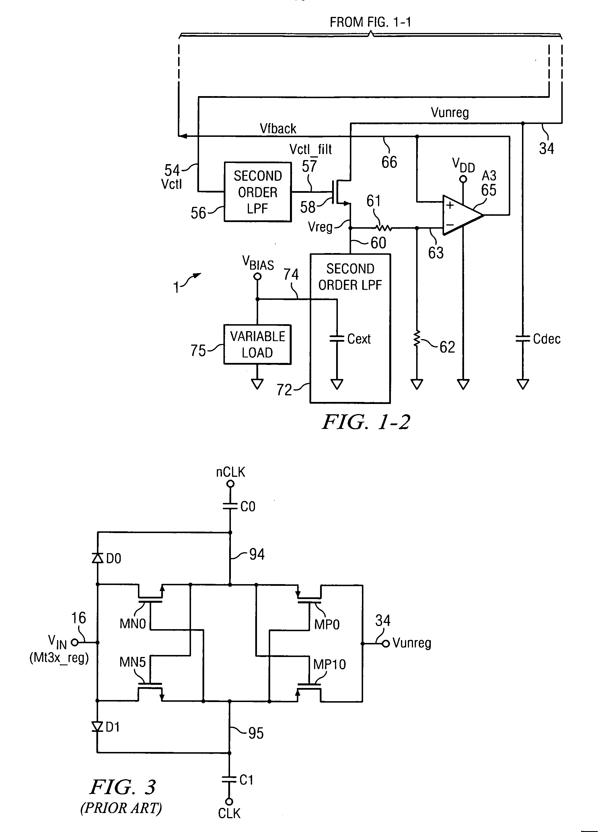
[0030]FIG. 1 illustrates a high voltage master / slave charge pump 1 which includes a master pump 2 which drives an external variable load and a slave pump 3 which drives a fixed internal load to regulate the output of the master pump 3. The unregulated output voltage Vunreg generated on output conductor 34 of master pump 2 is connected to the drain of a N-channel source-follower transistor 58. The source of source-follower transistor 58 is connected by conductor 60 to the input of a second order low pass filter (LPF) 72, the output 74 of which conducts a low-noise bias voltage VBIAS that is applied to a variable load 75. Vunreg may be subject to greater load-caused perturbations and / or noise than the output voltage Vctl produced by slave stage 3 because slave stage 3 has an essentially fixed load, rather than a variable load. The gate of source-follower transistor 58 is coupled by conductor 57 to the output of a second order LPF 56, the input of which is connected to the output 54 of...


PUM


Abstract

Charge pump circuitry (1) includes a master charge pump (2) including a voltage multiplier (5) and charge pump (30) which operate to produce a boosted, unregulated voltage (Vunreg), and also includes a slave charge pump (3) including a voltage multiplier (36) and charge pump (50) which operate to produce a boosted control voltage (Vctl) which then is filtered. The boosted, unregulated voltage (Vunreg) is regulated in response to the filtered, boosted control voltage (Vctl) to produce a boosted, regulated, low-noise voltage (Vreg). The boosted control voltage (Vctl), relative to a reference voltage (Vref_SH), is controlled by feedback circuitry (61,62,65) in response to the boosted, regulated, low-noise voltage (Vreg).

Description

BACKGROUND OF THE INVENTION[0001]The present invention relates generally to charge pump circuits, and more particularly to low noise, high multiplication factor charge pump circuits.[0002]“High multiplication factor” bias voltage generation in an integrated circuit is needed in many power-sensitive and cost-sensitive applications, including size-constrained systems for which large external components, such as inductors in various voltage boosting circuits, are prohibitive. Bias voltage generation circuitry for communication systems must be designed to meet stringent limitations on the generation and coupling of spurious RF noise levels into the RF components of the system. Also, high voltage multiplication or multiplier circuitry with very low spurious noise content within standard RF (radio frequency) communication frequency bands is needed to generate bias voltages and drive voltages for various applications, for example, to drive MEMS (microelectromechanical systems) actuators in...

Claims


Application Information

Patent Timeline
IPC IPC(8): G05F3/02
CPCH02M3/07
Inventor SHAY, MICHAEL J.IVANOV, VADIM V.
Owner TEXAS INSTR INC
Why Eureka
Try Eureka