Nickel silicide implementation for silicon-on-insulator (SOI) radio frequency (RF) switch technology

Inactive Publication Date: 2017-11-23
NEWPORT FAB
View PDF4 Cites 16 Cited by
  • Summary
  • Abstract
  • Description
  • Claims
  • Application Information

AI Technical Summary

Benefits of technology

[0014]In one embodiment, nickel silicide is also formed on the gate of the SOI CMOS transistor. As a result, the FET noise figure of the SOI CMOS transistor is relativ

Problems solved by technology

However, reducing the thickness TSi of silicon layer 203 results in significant challenges for process integration.
For RF switching technology in particular, this has several deleterious effects.
However, both of these approaches undesirably increase the parasitic off-state capacitance value COFF.
This permits the formation of thicker source/drain silicide regions 210 and 211, but significantly complicates the process flow, and may require additional capital investment for fabs that lack epitaxial deposition equipment.
Moreover, RSD integration is a challenging process to control in manufacturing, since small variations in conditions can result in poor epitaxial silicon quality.
Nickel-silicided SOI transistors fabricated using these advanced deep sub-micron processes are unable to meet the power handling requirements of an RF switc

Method used


Image

  • Nickel silicide implementation for silicon-on-insulator (SOI) radio frequency (RF) switch technology
  • Nickel silicide implementation for silicon-on-insulator (SOI) radio frequency (RF) switch technology
  • Nickel silicide implementation for silicon-on-insulator (SOI) radio frequency (RF) switch technology

Examples


Example

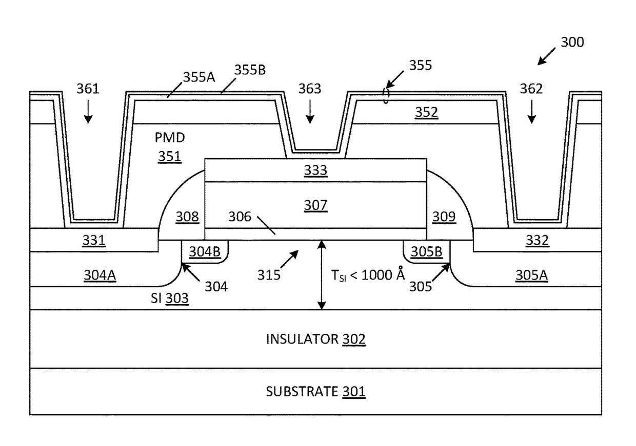
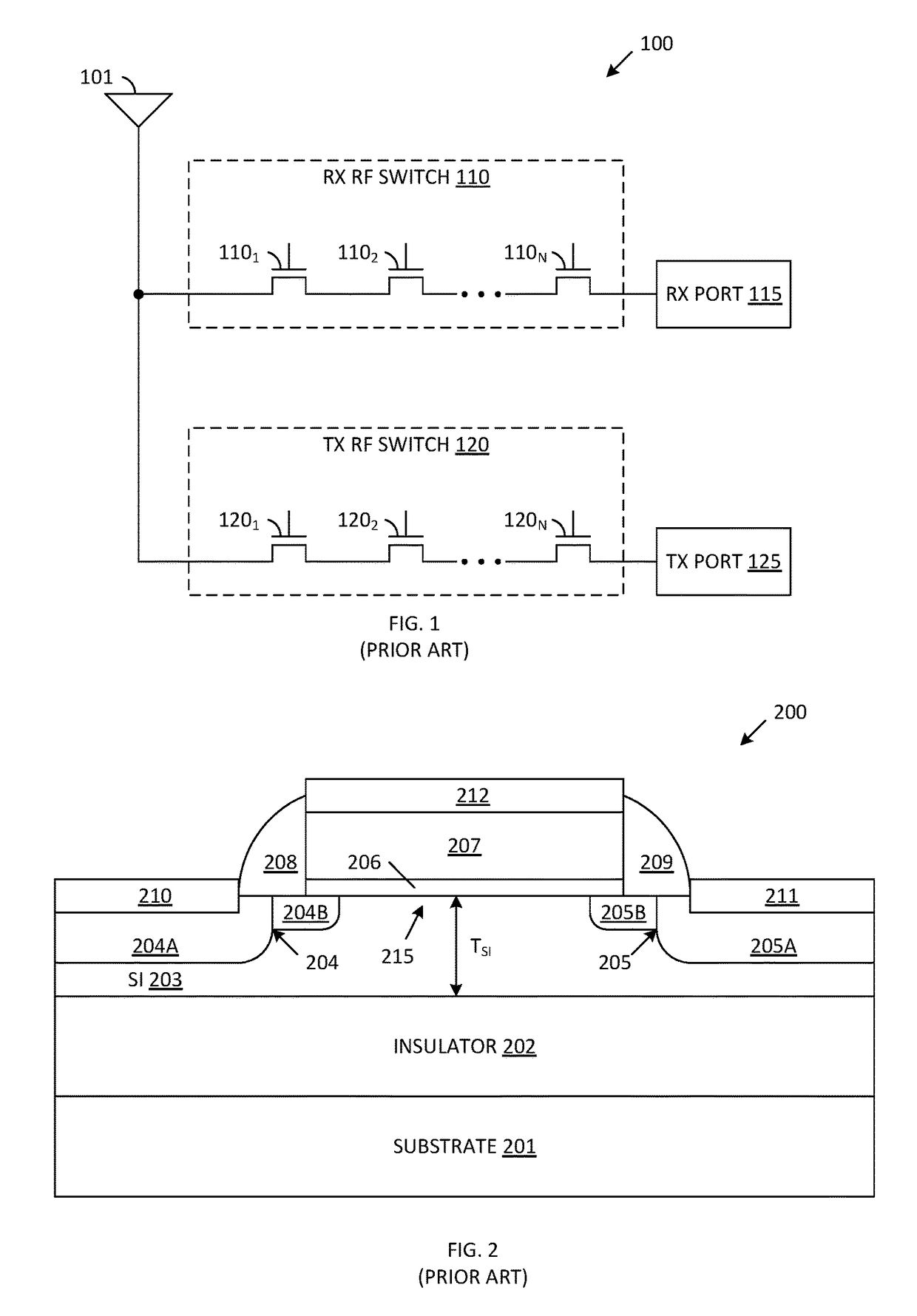
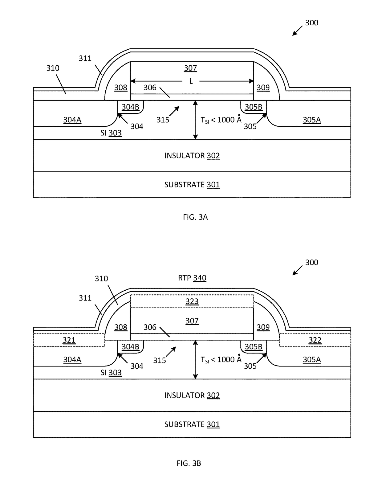
[0024]In general, the present invention implements an RF switch using a plurality of series-connected SOI CMOS transistors, each having a gate length of about 0.13 microns or more, and each having nickel silicide regions formed on their source and drain regions. Because each of the series-connected SOI CMOS transistors has a gate length of about 0.13 microns or more, these SOI CMOS transistors are capable of handling high RF powers, and exhibit the high breakdown voltages required to implement an RF switch. The nickel silicide regions advantageously contribute to a relatively a low on-resistance (RON) of the SOI CMOS transistors, while consuming a relatively small amount of the underlying silicon regions during their fabrication (when compared with the formation of titanium silicide or cobalt silicide). Thus, the nickel silicided SOI CMOS transistors of the present invention can be fabricated without raised source drain (RSD) integration. In addition, the SOI CMOS transistors of the...


PUM


Abstract

A radio frequency (RF) switch includes a plurality of series-connected silicon-on-insulator (SOI) CMOS transistors fabricated using a 0.13 micron (or larger) process, wherein the SOI CMOS transistors include nickel silicide formed on the source/drain regions. Each of the series-connected SOI CMOS transistors has a gate length of about 0.13 microns or more, thereby enabling these SOI CMOS transistors to handle high power RF signals, and exhibit the high breakdown voltages required to implement an RF switch. The nickel silicide regions advantageously contribute to a relatively a low on-resistance (RON) of the SOI CMOS transistors, while consuming a relatively small amount of the underlying silicon regions during their fabrication. The SOI CMOS transistors can be fabricated on a relatively thin silicon layer, thereby contributing to a relatively low off capacitance (COFF) of the SOI CMOS transistors. As a result, an RON*COFF value of the RF switch is advantageously minimized.

Description

FIELD OF THE INVENTION[0001]The present invention relates to the use of nickel silicide in connection with the fabrication of silicon-on-insulator (SOI) CMOS transistors having gate lengths of about 0.13 microns or greater, wherein the SOI CMOS transistors are used in high power applications such as radio frequency (RF) switching.RELATED ART[0002]FIG. 1 is a circuit diagram of a conventional radio frequency (RF) circuit 100, including an antenna 101, an RF receiver switch 110, an RF receiver port 115, an RF transmitter switch 120 and an RF transmitter port 125. RF receiver switch 110 includes a plurality of high-voltage field effect transistors (FETs) 1101-110N, which are connected in series (in a stack). The stack of high voltage FETs 1101-110N is controlled to route RF signals from antenna 101 to receive port 115. Similarly, RF transmitter switch 120 includes a stack of high-voltage FETs 1201-120N, which are controlled to route RF signals from transmit port 125 to antenna 101. As ...

Claims


Application Information

Patent Timeline
IPC IPC(8): H01L29/45H03K17/687H01L29/786H01L29/66H01L29/417H01L21/285H01L29/40H01L27/12H01L21/768H01L21/3105H04B1/38H01L29/423
CPCH01L29/458H01L27/1222H01L29/42384H01L29/41733H01L29/66772H04B1/38H01L21/31055H01L21/28518H01L21/76843H01L29/401H03K17/6872H01L29/78654H01L21/2855H01L29/665H03K17/102H03K17/693H04B1/48
Inventor HURWITZ, PAUL D.MOEN, KURT
Owner NEWPORT FAB
Why Eureka
Try Eureka