Method and apparatus for inspecting defect

a technology of defect detection and inspection method, applied in the direction of material analysis, optically investigating flaws/contamination, instruments, etc., to achieve the effect of reducing interference and improving the sensitivity of defect detection

Active Publication Date: 2013-05-09
HITACHI HIGH-TECH CORP
View PDF14 Cites 20 Cited by
  • Summary
  • Abstract
  • Description
  • Claims
  • Application Information

AI Technical Summary

Benefits of technology

[0028]According to the aspects of the present invention, the above-described configurations enable to obtain effects in which the sensitivity of defect detection can be improved by reducing interference due to multiple interference of an oxide film and surface roughness of a metal film, the inspection speed same as that of a conventional system using laser illumination can be realized by high-brightness broadband illumination, and the above-described performance can be realized by a simple optical system.

Problems solved by technology

Especially, with advanced fine patterning, detection of finer defects is required in an inspection for a semiconductor wafer, and extracting a weak detected light beam from fine defects while being distinguished from background light noise is a major challenge in an inspection technique.

Method used


Image

  • Method and apparatus for inspecting defect
  • Method and apparatus for inspecting defect
  • Method and apparatus for inspecting defect

Examples


first embodiment

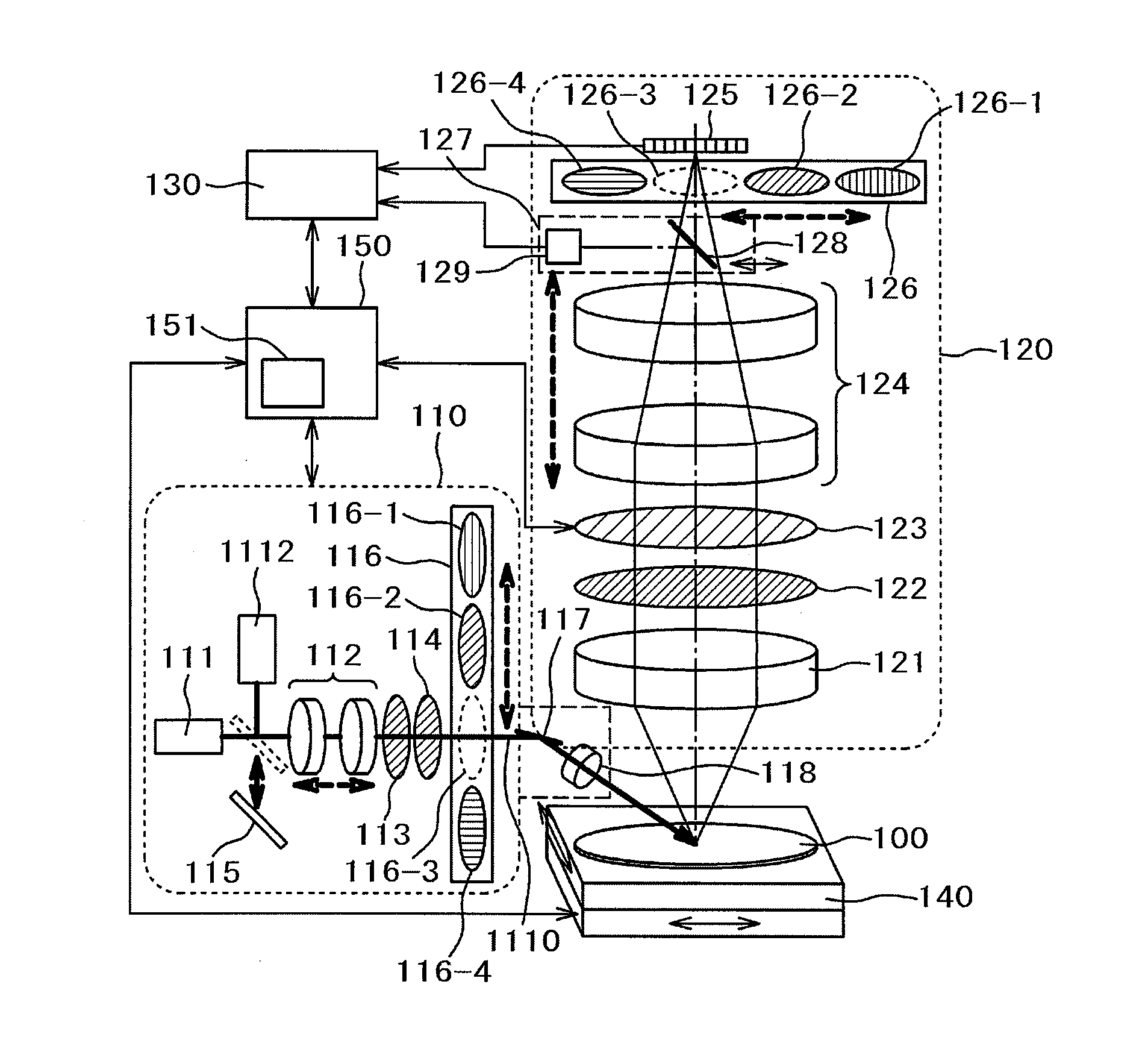
[0041]An example of applying the present invention to a dark-field illumination-type semiconductor wafer defect inspection apparatus is shown in a first embodiment. A basic configuration of the semiconductor wafer inspection apparatus according to the embodiment will be described on the basis of FIG. 1A.

[0042]The semiconductor wafer inspection apparatus shown in FIG. 1A includes an illumination optical system 110, a detection optical system 120, an image processing unit 130, a stage unit 140 on which a semiconductor wafer (substrate) 100 as a sample is mounted, and a control unit 150 that controls the entire apparatus.

[0043]In the illumination optical system 110 of FIG. 1A, the reference numeral 1112 denotes a high-coherent broadband light source. The illumination light source is switched between a laser light source 111 and the high-coherent broadband light source 1112 by a switching mirror 115 in accordance with a target and object of the inspection.

[0044]The polarization of an il...

second embodiment

[0066]FIG. 8 is an explanatory diagram of a second embodiment of the present invention.

[0067]In addition to the configuration of the first embodiment of the present invention described using FIG. 1, an optical path branch mechanism 1211 (half mirror or the like) is provided on the objective lens 121 of a detection optical system 1201 in FIG. 8. While a first detection system includes optical systems 122 to 126 as similar to the case of the first embodiment, a second detection system branched at the optical path branch mechanism 1211 includes second optical filtering means (a polarization filter 1221, a spatial filter 1231, and a wavelength selecting element unit 1261), a second imaging lens 1241, and a second image sensor 1251. Further, the second optical filtering means of the second detection system can be controlled independently from the first optical filtering means (the polarization filter 122, the spatial filter 123, and the wavelength selecting element unit 126) of the first...

third embodiment

[0071]FIG. 9 is a diagram for showing a configuration of a semiconductor wafer inspection apparatus in a third embodiment of the present invention. In the embodiment, in addition to the configuration of the semiconductor wafer inspection apparatus described using FIG. 1 in the first embodiment, a second detection optical system 1202, namely, a second objective lens 1212, second optical filtering means (a polarization filter 1222, a spatial filter 1232, and a wavelength selecting element 1262), a second imaging lens 1242, and a second image sensor 1252 are provided. The configuration and function of the illumination optical system 110 are the same as those described in the first embodiment.

[0072]As similar to the second embodiment, the second optical filtering means can be controlled independently from the first optical filtering means (the polarization filter 122, the spatial filter 123, and the wavelength selecting element 126) of the first detection optical system 120.

[0073]In thi...


PUM

PropertyMeasurementUnit
defect inspectionaaaaaaaaaa
wavelengthaaaaaaaaaa
electricallyaaaaaaaaaa

Abstract

In inspecting a substrate having a transparent oxide film or a metal film formed on a surface thereof by using a dark field type inspection apparatus installing a laser light source, an illuminating beam having a high coherence causes variations in reflection strength due to multiple interferences within the transparent oxide film or an interference of scattered beams due to the surface roughness of the metal film occurs and which leads to degradation in the sensitivity of defect detection. The present invention solves the problem by providing a low-coherence but high-brightness illumination using a highly directive broadband light source, and a system in which the conventional laser light source is simultaneously employed to selectively use the light sources, thereby enabling a highly sensitive inspection according to the condition of a wafer.

Description

TECHNICAL FIELD[0001]The present invention relates to an inspection technique of detecting defects on an inspection target on the surface of which a pattern is formed on the basis of image information obtained using a light beam, and particularly to an inspection technique of detecting fine defects in which a substrate with a pattern such as a semiconductor wafer is used as an inspection target.BACKGROUND ART[0002]In a defect inspection for a substrate with a pattern, the sensitivity of defect detection is largely affected depending on how a detected light beam from defects can be detected while being distinguished from a detected light beam (background light noise) from a pattern or a base film. Especially, with advanced fine patterning, detection of finer defects is required in an inspection for a semiconductor wafer, and extracting a weak detected light beam from fine defects while being distinguished from background light noise is a major challenge in an inspection technique.[00...

Claims


Application Information

Patent Timeline
Patent Type & Authority Applications(United States)
IPC IPC(8): G01N21/95
CPCG01B11/303G01N21/21G01N21/956G01N21/9501G01N21/94
Inventor MATSUMOTO, SHUNICHIUENO, TAKETOTANIGUCHI, ATSUSHI
Owner HITACHI HIGH-TECH CORP
Why Eureka
Try Eureka