Laminated wiring board and manufacturing method for same
- Summary
- Abstract
- Description
- Claims
- Application Information
AI Technical Summary
Benefits of technology
Problems solved by technology
Method used
Image
Examples
first embodiment
[0032]
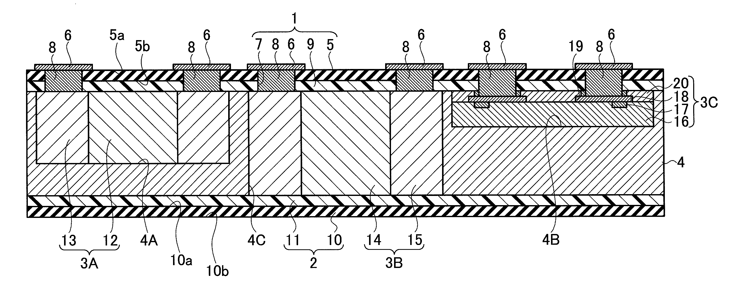
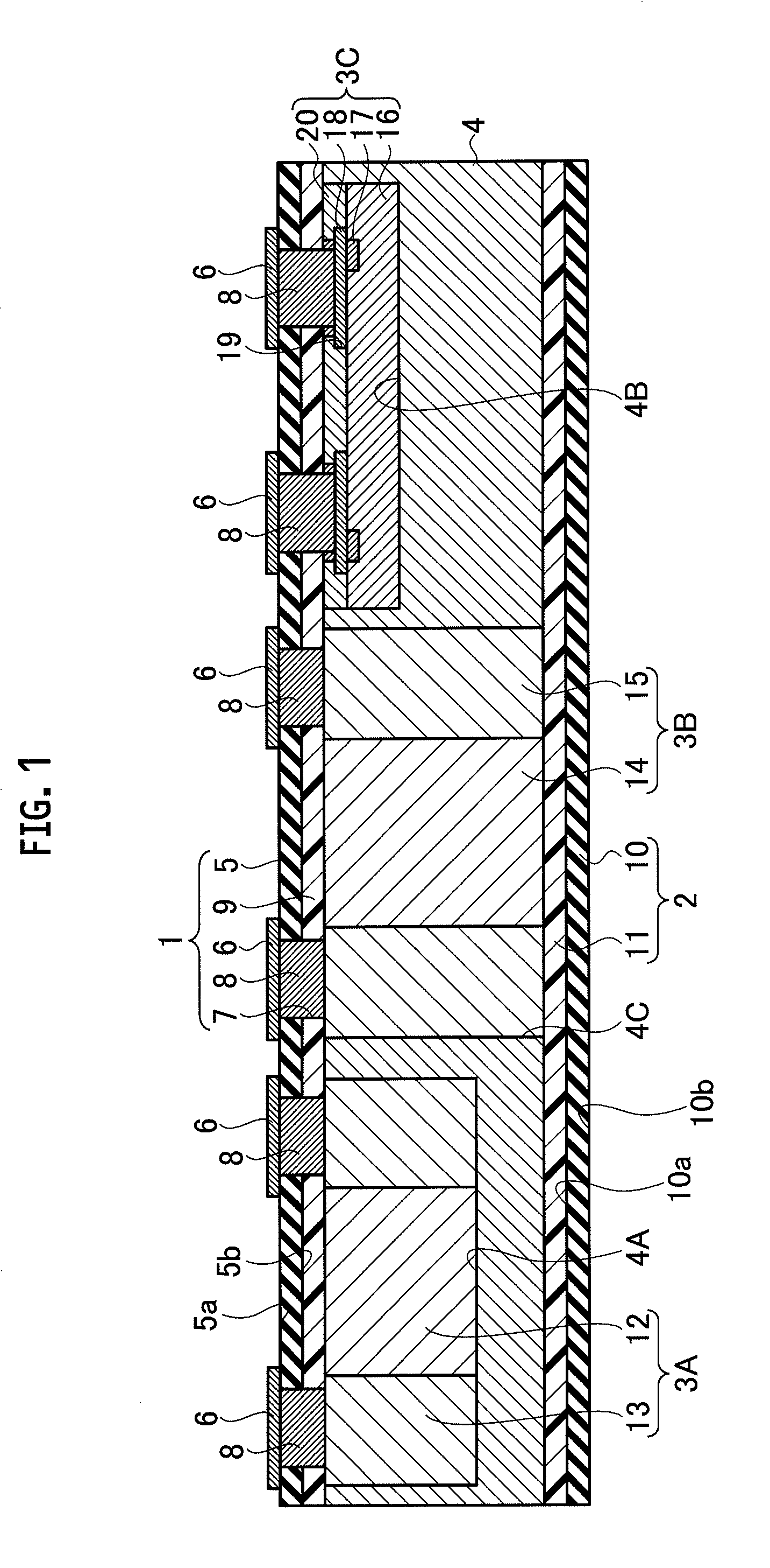
[0033]First, a configuration of a laminated wiring board to which the present invention is applied will be explained with reference to FIG. 1. FIG. 1 is a sectional view of a laminated wiring board according to a first embodiment of the present invention. The laminated wiring board according to the first embodiment of the present invention includes mainly a first substrate 1, a second substrate 2, a plurality of electronic components 3 (3A, 3B, and 3C) having different heights and embedded between the first substrate 1 and the second substrate 2, and an insulating embedding member 4 in which the electronic components 3 are embedded. It is to be noted that the number of the electronic components 3 may be one, instead of more than one.
[0034]The first substrate 1 has an insulating layer 5 made of, for example, a polyimide resin film. On one surface 5a of the insulating layer 5, conductor circuits 6 made of copper foil are formed. On the other surface 5b of the insulating layer 5,...
second embodiment
[0080]In the first embodiment of the present invention, the case was explained where the electronic components were embedded by the prepreg that is used as the embedding member, but, in a second embodiment of the present invention, a case will be explained where an electronic component is embedded by using an embedding member having a laminated structure of an insulating layer and an adhesive layer.
[0081]
[0082]As illustrated in FIG. 10, a laminated wiring board according to the second embodiment of the present invention includes a first substrate 21, a second substrate 31, an electronic component 60 embedded between the first substrate 21 and the second substrate 31, an embedding member 41 in which the electronic component 60 is embedded.
[0083]In the first substrate 21, conductor circuits 24 are formed on an upper face of an insulating layer 22, and an adhesive layer 23 is formed on a lower face of the insulating layer 22. Conductors (vias) 25 are respectively formed in a plurality ...
PUM
| Property | Measurement | Unit |
|---|---|---|
| Electrical conductor | aaaaa | aaaaa |
| Height | aaaaa | aaaaa |
Abstract
Description
Claims
Application Information


