Input display device

a display device and display technology, applied in the field of input display devices, can solve problems such as display defect or malfunction, and achieve the effect of reducing the occurrence of display defect and occurren

Active Publication Date: 2013-05-16
NITTO DENKO CORP
View PDF17 Cites 26 Cited by
  • Summary
  • Abstract
  • Description
  • Claims
  • Application Information

AI Technical Summary

Benefits of technology

[0008]An object of the invention is to provide an input display device capable of reducing occurrence of a display defect and occurrence of malfunctioning without loosing a natural operation feel.
[0013]According to the invention, a antistatic layer having a surface resistance value of 1.0×10⁹ to 1.0×10¹¹Ω / □ is disposed between a liquid crystal layer containing liquid crystal molecules that are homogeneously aligned in an absence of an electric field and a first polarizer. Thus, the charging of the first polarizer due to a static electricity or the like can be suppressed and misalignment of the liquid crystal molecules in the liquid crystal layer can be suppressed. Further, with the surface resistance value being within the aforementioned range, the capacitive sensor can accurately sense a change in the electric capacitance produced between the transparent electrode pattern and the user's finger. Therefore, it is possible to reduce occurrence of the display defect as well as occurrence of the malfunctioning, without impairing a natural feel of operation.

Problems solved by technology

However, with the capacitive type, in a case where a liquid crystal layer containing liquid crystal molecules that are homogeneously aligned in an absence of an electric field is used as a liquid crystal layer and a capacitive sensor is used as a touch sensor, there is a problem that a display defect or malfunctioning may occur often.

Method used


Image

  • Input display device
  • Input display device
  • Input display device

Examples


example 1

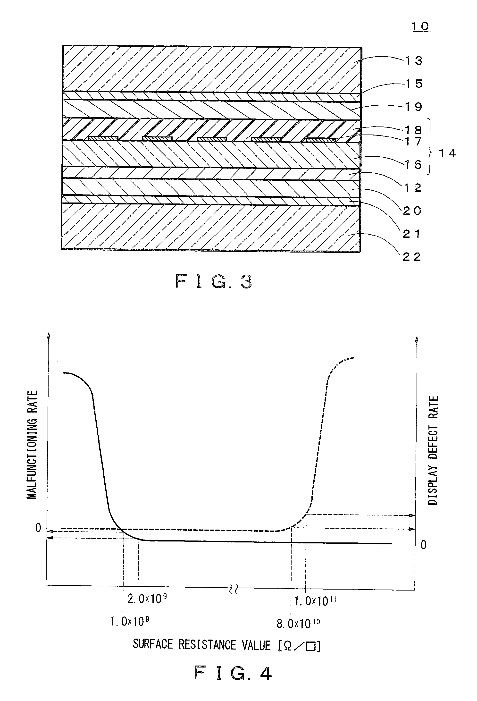
[0053]First, a coloring-purpose resin layer was formed on one side of a glass substrate by applying a coloring-purpose resin solution in which pigments are dispersed, and a transparent electrode layer was formed on the other side of the glass substrate by forming a film of indium tin oxide by sputtering. Thereafter, an upper substrate having a color filter and a transparent electrode pattern was fabricated by etching the coloring-purpose resin layer and the transparent electrode layer, respectively.

[0054]Further, a thin-film transistor, a scan line, a signal line and a pixel electrode were formed on a separate glass substrate to form a lower substrate.

[0055]Next, a polyimide alignment film was formed on a color filter side of the upper substrate and a pixel electrode side of the lower substrate, and rubbed in one direction with a rubbing cloth. After spreading spherical fine particles on the lower substrate, the lower substrate and the upper substrate were laid on top of each other ...

example 2

[0058]An input display device was fabricated that has a structure similar to that of Example 1, except that the antistatic layer having a surface resistance value of 8.0×10¹⁰Ω / □ was used. An acrylic pressure sensitive adhesive agent (thickness of 25 μm), in which bis(trifluoromethanesulfonyl)imide lithium is dispersed at 2 weight % against the total weight of the antistatic layer was used as the antistatic layer.


PUM


Abstract

An input display device includes a liquid crystal layer containing liquid crystal molecules that are homogeneously aligned in an absence of an electric field, a first polarizer disposed on a viewing side of the liquid crystal layer, a capacitive sensor disposed between the first polarizer and the liquid crystal layer, and an antistatic layer disposed between the first polarizer and the capacitive sensor, the antistatic layer being attached to the first polarizer. The capacitive sensor has a transparent substrate, a transparent electrode pattern formed on the transparent substrate, and a first adhesive layer formed on the transparent substrate to embed the transparent electrode pattern, and the antistatic layer has a surface resistance value of 1.0×10⁹ to 1.0×10¹¹Ω / □.

Description

CROSS REFERENCE TO RELATED APPLICATIONS[0001]This application claims the benefit of Japanese Application No. 2011-250902, filed Nov. 16, 2011, which is hereby incorporated by reference herein in its entirety.BACKGROUND OF INVENTION[0002]1. Field of the Invention[0003]The present invention relates to an input display device that is capable of inputting information by a touch with a finger, a stylus pen or the like.[0004]2. Background of the Invention[0005]In the related art, there are some input display apparatuses, such as mobile equipments provided with a liquid crystal panel as a display, that have a touch panel mounted on a display screen of the display to satisfy the need for a reduced size or thickness and put into practical use. There are various types of touch panels such as a capacitive type, a resistive film type, an optical type, an ultrasonic type, and an electromagnetic induction type.[0006]For example, an inner touch panel-type input display device has been proposed in ...

Claims


Application Information

Patent Timeline
Patent Type & Authority Applications(United States)
IPC IPC(8): G06F3/044
CPCG06F3/044G02F1/13338G02F2202/22G02F2001/133738G06F3/0412G06F3/0443G02F1/133738
Inventor ISHIBASHI, KUNIAKISUGINO, AKIKOCHIBA, TSUYOSHIFUJITA, MASAKUNIYAMAOKA, TAKASHI
Owner NITTO DENKO CORP
Why Eureka
Try Eureka