Lateral double diffusion metal-oxide semiconductor device and method for manufacturing the same

a metal-oxide semiconductor and lateral double diffusion technology, applied in the direction of semiconductor devices, basic electric elements, electrical appliances, etc., can solve the problems of increasing the breakdown voltage without increasing the on-resistance, the entire process becomes more complicated and expensive than most in the industry, and the breakdown voltage cannot achieve both high breakdown voltage and low on-resistance, so as to reduce the concentration of electric fields, increase the doping concentration of the n-drift region, and reduce the complexity of operation

Active Publication Date: 2013-05-23
HYUNDAI MOTOR CO LTD
View PDF0 Cites 10 Cited by
  • Summary
  • Abstract
  • Description
  • Claims
  • Application Information

AI Technical Summary

Benefits of technology

[0018]Advantageously, when an n-drift region is formed on a P-type substrate, a p-body is epitaxially formed on the n-drift region, and then the p-body region is partially etched to form a plurality of p-epitaxial layers, so that when the semiconductor device in the illustrative embodiment of the present invention performs a reverse voltage blocking operation, one or more depletion layers are formed between the junction surfaces of the p-epitaxial layers and the n-drift region, as well as between the junction surfaces of the n-drift region and the p-body. As a result, it is possible to reduce an electric field concentrated to a gate oxide film while at the same time decreasing the complexity of the operation.
[0019]In addition, since it is possible to increase the doping concentration of the n-drift region, to the illustrative embodiment of the present invention also lowers an ON-resistance produced when the inventive semiconductor device performs a forward operation.

Problems solved by technology

However, the above-mentioned conventional power devices cannot realize both of the high breakdown voltage and low ON-resistance.
As a result, with such a conventional LDMOS transistor structure, it is difficult to increase the breakdown voltage without increasing the ON-resistance.
However, due to the rather complicated steps involved in the above process, such as
CMP, required for forming such a trench structure, the entire process becomes more complicated an expensive that most in the industry would desire.

Method used


Image

  • Lateral double diffusion metal-oxide semiconductor device and method for manufacturing the same
  • Lateral double diffusion metal-oxide semiconductor device and method for manufacturing the same
  • Lateral double diffusion metal-oxide semiconductor device and method for manufacturing the same

Examples


Embodiment Construction

[0027]Hereinafter reference will now be made in detail to various embodiments of the present invention, examples of which are illustrated in the accompanying drawings and to described below.

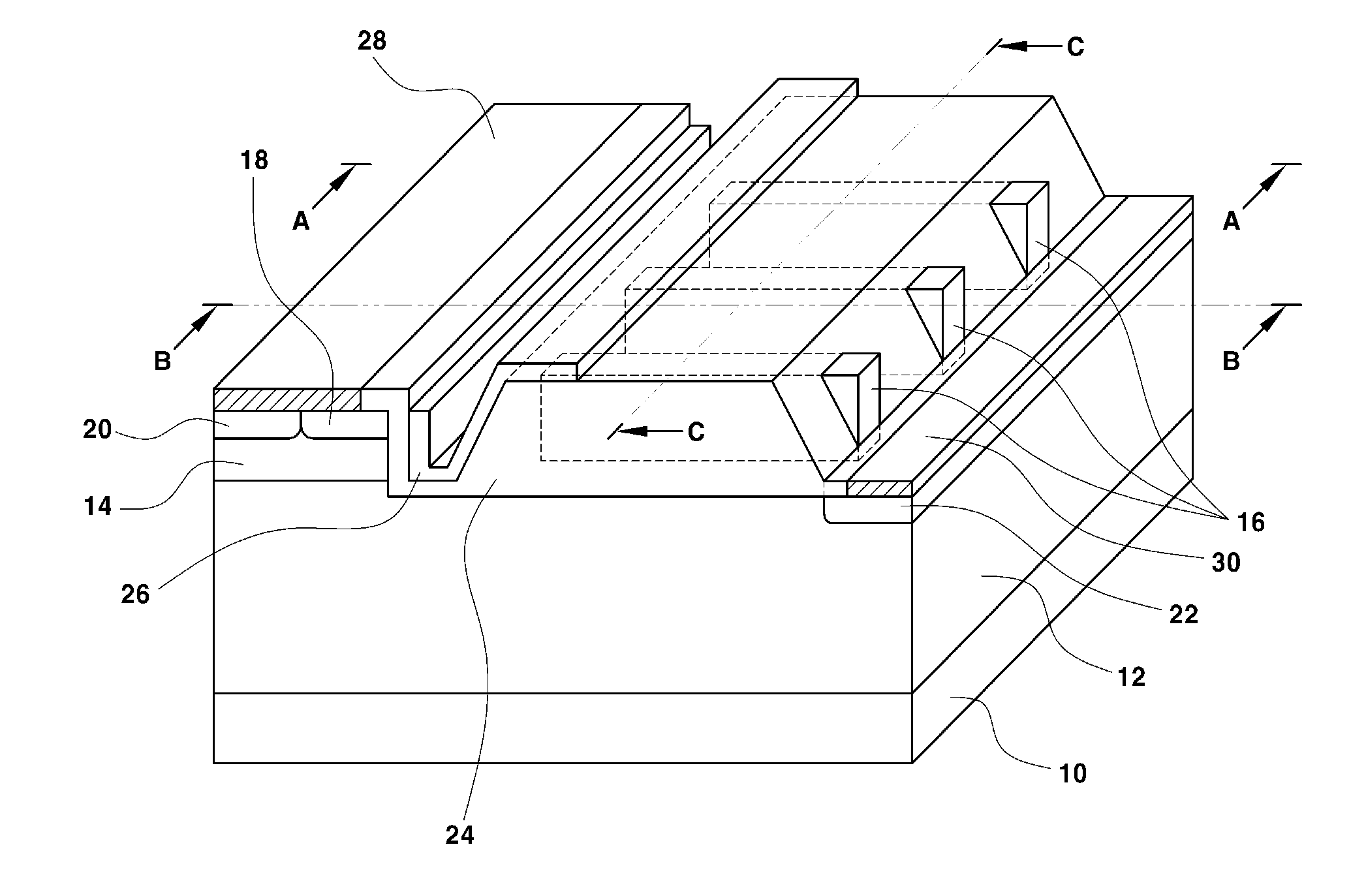
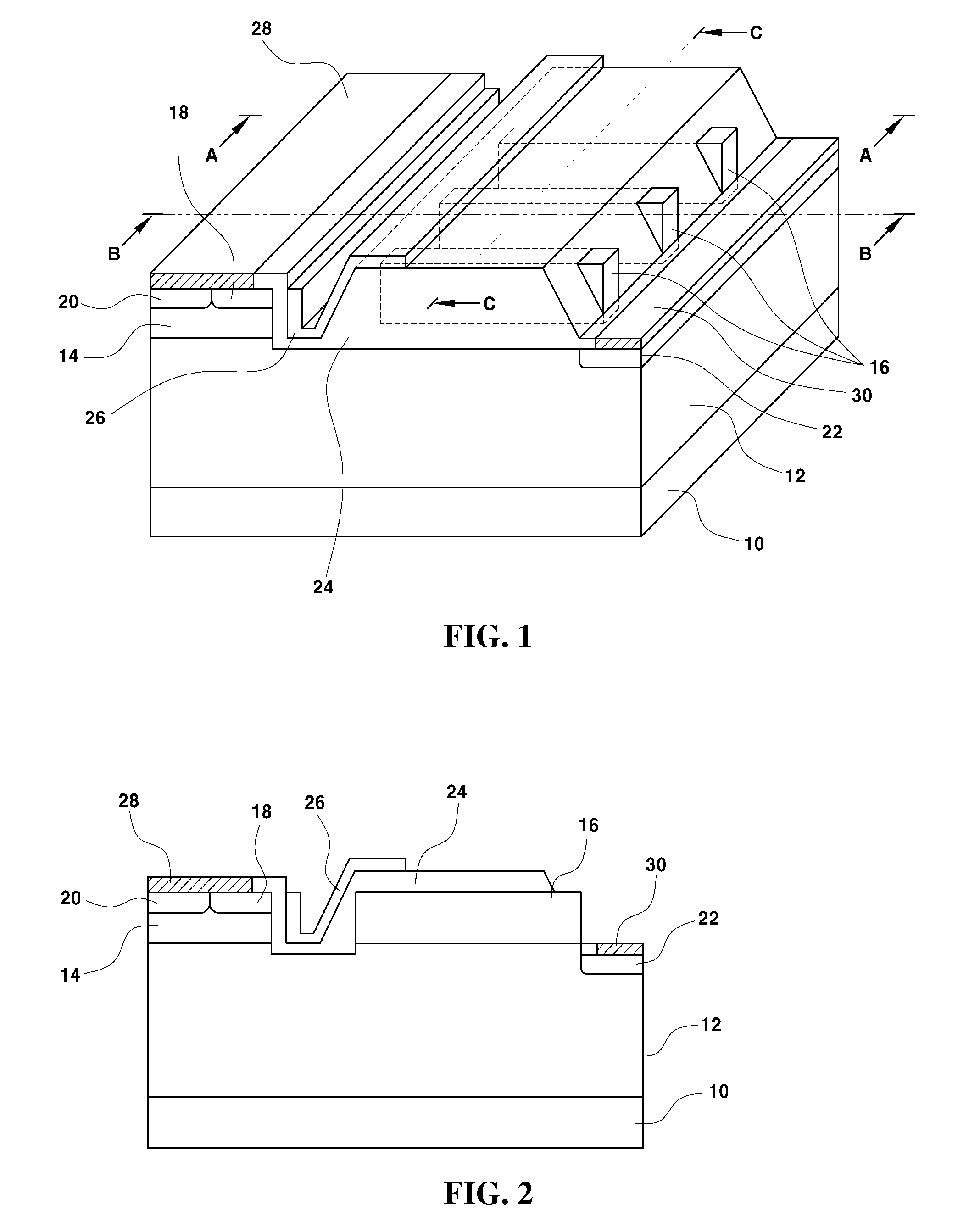
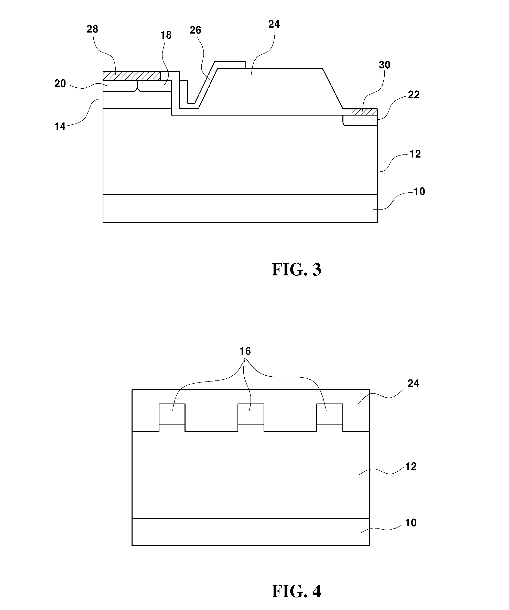
[0028]First, a method for manufacturing a silicon carbide lateral MOSFET device will be described with reference to FIG. 5 to help the understanding of the present invention. When an n-drift region used as a drift region is formed on a single crystal semiconductor substrate, i.e., a P-type substrate 10, a p-body 14 is epitaxially formed on the n-drift region 12 (see FIG. 5a). Next, the p-body 14 is etched in a comb shape using a conventional etching process to form a plurality of p-epitaxial layers 16 in the p-body 14. The p-body 14 and the p-epitaxial layers 16 are spaced apart from each other in the widthwise direction, and the p-epitaxial layers 16 are spaced apart from each other in the longitudinal direction (see FIGS. 1 and 5b).

[0029]Next, N-type and P-type ions are implanted to the p-body ...


PUM


Abstract

Disclosed is an LDMOS device, which is configured to reduce an electric field concentrated to a gate oxide film and lower an ON-resistance produced when the device conducts a forward action, and a method for manufacturing the same. More specifically, when an n-drift region is formed on a P-type substrate, a p-body is formed on the n-drift region through an epitaxial process, and then the p-body region is partially etched to form a plurality of p-epitaxial layers, so that when the device executes an action for blocking a reverse voltage, depletion layers are formed between the junction surfaces of the p-epitaxial layers and the n-drift region including the junction surfaces between the n-drift region and the p-body.

Description

CROSS-REFERENCE TO RELATED APPLICATION[0001]This application claims under 35 U.S.C. §119(a) the benefit of Korean Patent Application No. 10-2011-0122075 filed on Nov. 22, 2011, the entire contents of which are incorporated herein by reference.BACKGROUND[0002](a) Technical Field[0003]The present invention relates to a Lateral Double Diffusion Metal-Semiconductor (LDMOS) device, and a method for manufacturing the same. More particularly, the present invention relates to an LDMOS device, which is configured to reduce an electric field concentrated to a gate oxide film, and lower ON-resistance produced when the device conducts a forward action, and a method for manufacturing the same.[0004](b) Background Art[0005]Recently, as devices and application appliances employing one or more power semiconductor devices tend to become bigger and larger in terms of size and capacitance, there has been high demand for power semiconductor devices, such as an Insulated Gate Bipolar Transistor (IGBT) o...

Claims


Application Information

Patent Timeline
Patent Type & Authority Applications(United States)
IPC IPC(8): H01L29/78
CPCH01L29/1608H01L29/42368H01L29/0657H01L29/7825H01L29/0634H01L29/66068H01L29/7816
Inventor LEE, JONG SEOKHONG, KYOUNG KOOK
Owner HYUNDAI MOTOR CO LTD
Why Eureka
Try Eureka