Fabrication method of electrochromic device
- Summary
- Abstract
- Description
- Claims
- Application Information
AI Technical Summary
Benefits of technology
Problems solved by technology
Method used
Image
Examples
Embodiment Construction
[0032]The advantages and features of the present invention will be fully understood by reference to the following two examples in conjunction with the accompanying drawings.
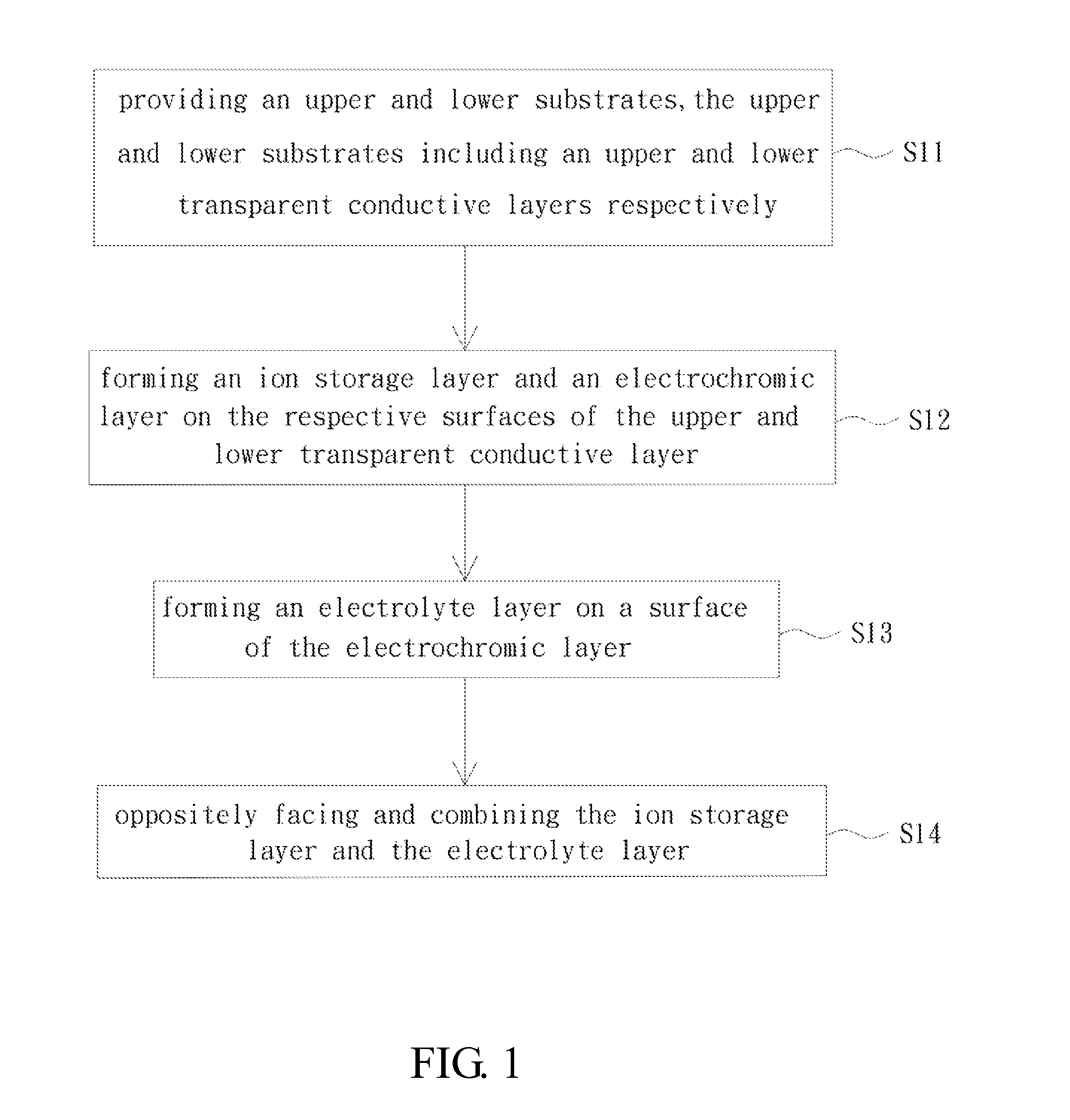
[0033]FIG. 1 is a flow chart of a fabrication method of an electrochromic device according to a preferred embodiment of the present invention; and
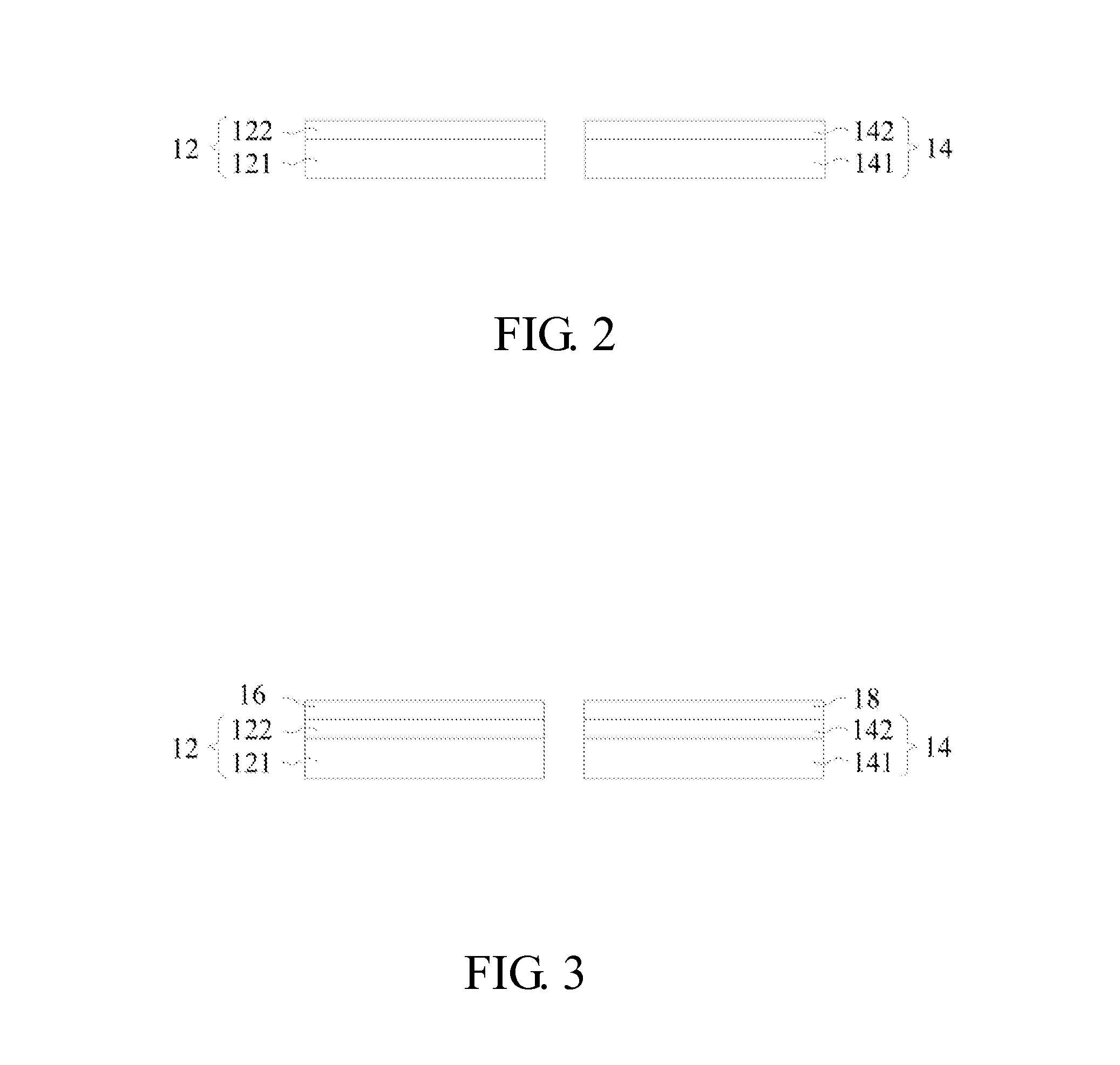
[0034]FIGS. 2-6 are views showing a process of fabricating an electrochromic device according to a preferred embodiment of the present invention.
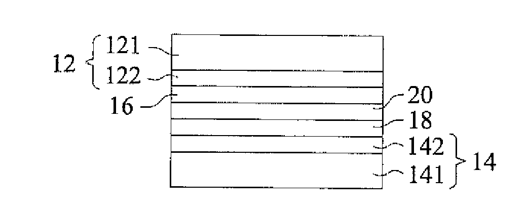
[0035]As shown in FIGS. 1 and 2, in step S11, an upper substrate 12 and a lower substrate 14 are provided, wherein the upper substrate 12 includes an upper base layer 121 and an upper transparent conductive layer 122, and the lower substrate 14 includes a lower base layer 141 and a lower transparent conductive layer 142. The upper base layer 121 and the lower base layer 141 may be made of glass, plastics or metal. The metal may be aluminum, chromium, silver or nickel, and has a thickness of 1 um-100 um. The upper transparent co...
PUM
| Property | Measurement | Unit |
|---|---|---|
| Temperature | aaaaa | aaaaa |
| Temperature | aaaaa | aaaaa |
| Temperature | aaaaa | aaaaa |
Abstract
Description
Claims
Application Information


