Optoelectronic Component

a technology of optoelectronic components and components, applied in the direction of basic electric elements, electrical equipment, semiconductor devices, etc., can solve the problems of no known optoelectronic components which make available light, and achieve the effects of reducing absorption losses, preventing absorption losses, and reducing absorption losses

Active Publication Date: 2013-06-06
OSRAM OLED
View PDF4 Cites 32 Cited by
  • Summary
  • Abstract
  • Description
  • Claims
  • Application Information

AI Technical Summary

Benefits of technology

[0020]In a preferred embodiment, the semiconductor chips are embodied as surface emitters, in particular as thin-film chips. These semiconductor chips are cast up to the level of their active layers in silicone filled with titanium dioxide, TiO2, having a reflectivity of greater than 95%. Alternatively, the silicone can also be filled with ZrO2, Al2O3 or ZnO. The use of highly reflective filled silicone is particularly advantageous since this prevents absorption losses as a result of exposed regions of the carrier. Alternatively, the carrier surface facing the semiconductor chips can be coated with a reflection layer, in particular composed of silver, which likewise reduces the absorption losses.
[0021]In a preferred embodiment, the diffusing layer has the form of a lens. This is particularly advantageous since a broader emission characteristic results in comparison with the diffusing layer having a homogeneous thickness, that is to say without a lens form. In other words, more light leaves the optoelectronic component at greater angles, preferably at angles of greater than 60 degrees, particularly preferably at an angle of greater than 90 degrees. The greater the angles at which the light is emitted by the optoelectronic component, the more efficiently the mixed light ...

Problems solved by technology

In particular, there are no known optoelectronic components which make avai...

Method used


Image

  • Optoelectronic Component
  • Optoelectronic Component
  • Optoelectronic Component

Examples


Embodiment Construction

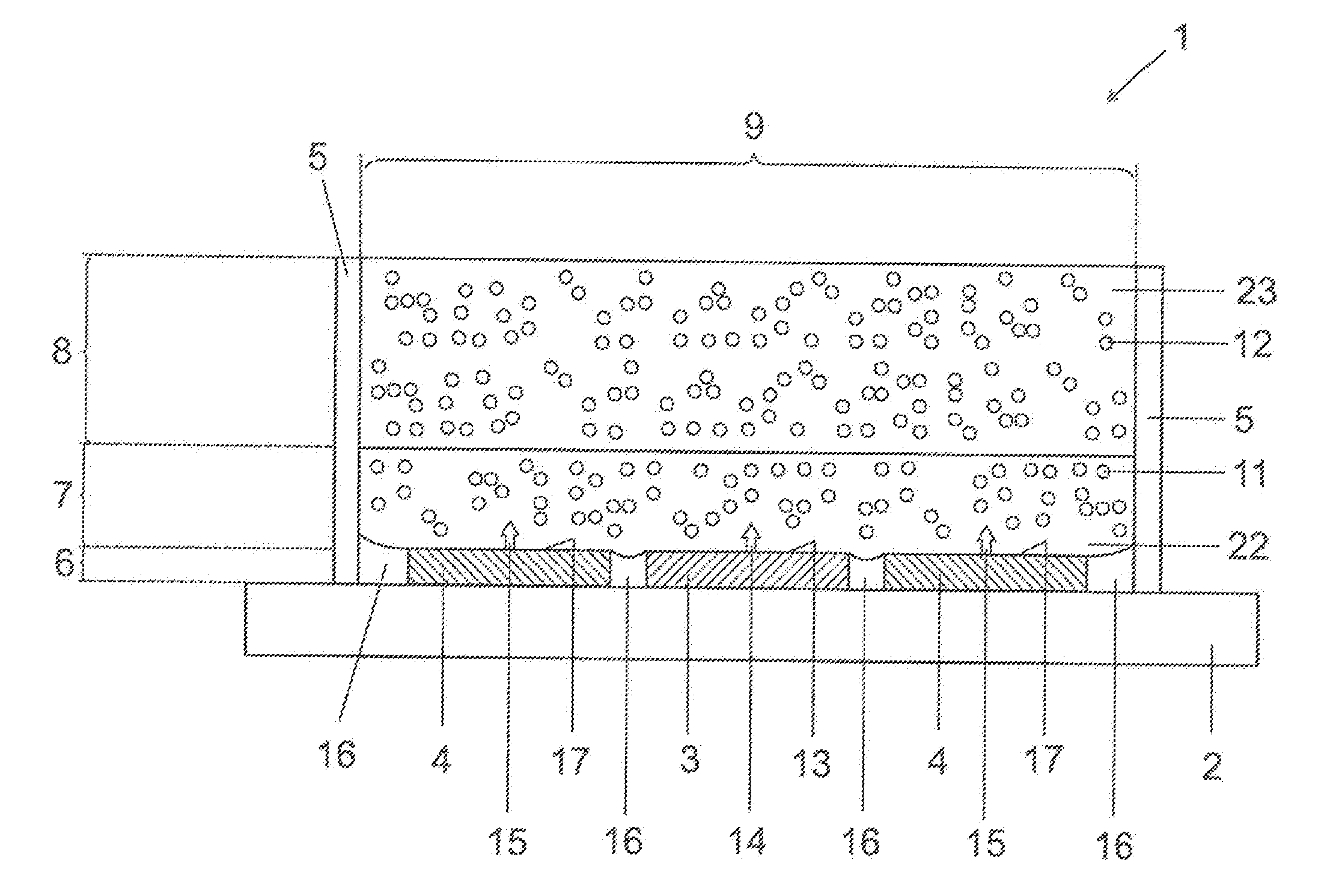
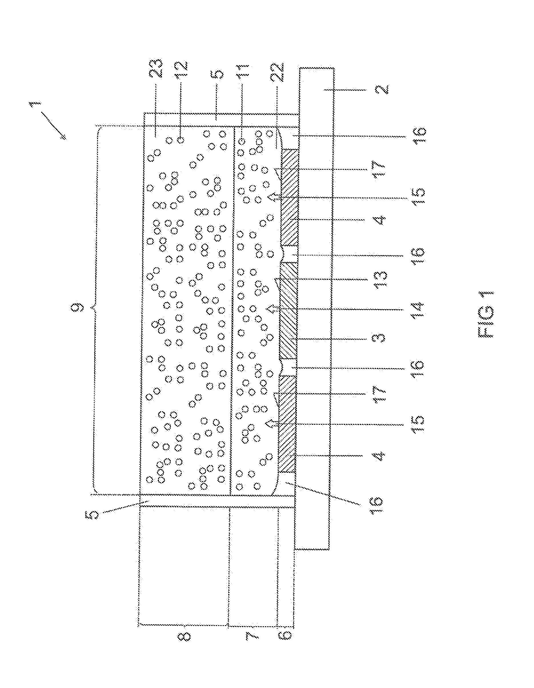
[0039]FIG. 1 shows a sectional view through an optoelectronic component 1. The optoelectronic component 1 serves for mixing electromagnetic radiation having different wavelengths, in particular in the far field. A first semiconductor chip 3 having a first radiation exit surface 13 for emitting electromagnetic radiation in a first spectral range 14 is provided on a carrier 2. Two further semiconductor chips 4 having a second radiation exit surface 17 for emitting electromagnetic radiation in a second spectral range 15 are provided on the carrier 2.

[0040]The semiconductor chips 3, 4 lie in one plane, the semiconductor chip plane 6. The height of said semiconductor chip plane 6 is between 0.05 mm and 0.3 mm, preferably approximately 0.2 mm. A diffusing layer 8 is provided on the first and second radiation exit surfaces 13, 17 of the semiconductor chips 3, 4 which face away from the carrier 2. Scattering particles 12, in particular aluminum dioxide, silicon dioxide or titanium dioxide, ...


PUM


Abstract

An optoelectronic component can be used for mixing electromagnetic radiation having different wavelengths, in particular in the far field. The optoelectronic component includes a carrier. A first semiconductor chip has a first radiation exit surface for emitting electromagnetic radiation in a first spectral range is provided on the carrier and a second semiconductor chip as a second radiation exit surface for emitting electromagnetic radiation in a second spectral range is provided on the carrier. A diffusing layer is provided on the radiation exit surfaces of the semiconductor chips which face away from the carrier.

Description

[0001]This application is a continuation of co-pending International Application No. PCT / EP2011 / 062598, filed Jul. 22, 2011, which designated the United States and was not published in English, and which claims priority to German Application No. 10 2010 038 396.1, filed Jul. 26, 2010, both of which applications are incorporated herein by reference.TECHNICAL FIELD[0002]The present invention relates to an optoelectronic component for mixing electromagnetic radiation having different wavelengths.BACKGROUND[0003]In order to generate mixed light from electromagnetic radiation of different semiconductor chips, light boxes have been used heretofore. With the aid of the light boxes, it is only possible to generate far fields with a relatively narrow angular distribution of the intensity. In particular, there are no known optoelectronic components which make available light already mixed to the greatest possible extent at their output facets.SUMMARY OF THE INVENTION[0004]In one aspect, the i...

Claims


Application Information

Patent Timeline
IPC IPC(8): H01L33/30
CPCH01L25/0753H01L33/50H01L33/56H01L33/60H01L2933/0091H01L2924/0002H01L33/30H01L2924/00H01L33/32H01L33/54H01L33/58H01L27/15H01L33/483H01L33/502
Inventor WIRTH, RALPHLINKOV, ALEXANDER
Owner OSRAM OLED
Why Eureka
Try Eureka