Gain coupling distributed feedback type semiconductor laser and manufacturing method thereof

A distributed feedback, gain coupling technology, applied in the semiconductor field, can solve the problems of unstable laser output mode, unable to achieve pure gain coupling, affecting laser performance, etc., to avoid dual-mode lasing, avoid refractive index coupling effect, avoid The effect of absorbing losses

Pending Publication Date: 2021-10-22
SUZHOU UNIV
View PDF5 Cites 0 Cited by
  • Summary
  • Abstract
  • Description
  • Claims
  • Application Information

AI Technical Summary

Problems solved by technology

There are different defects in the above methods: etching and ion implantation will introduce a large number of defects, which will affect the performance of the laser; the methods of epitaxially growing the active layer, making absorption gratings and "conductivity type inversion" gratings are inevitable. The refractive index grating produces a refractive index coupling effect, so pure gain coupling cannot be achieved, and dual-mode lasing will also occur, resulting in an unstable output mode of the laser; the common defect of the above three methods is that grating preparation is required, and the manufacturing process Complicated and expensive to manufacture

Method used


Image

  • Gain coupling distributed feedback type semiconductor laser and manufacturing method thereof
  • Gain coupling distributed feedback type semiconductor laser and manufacturing method thereof
  • Gain coupling distributed feedback type semiconductor laser and manufacturing method thereof

Examples


Embodiment Construction

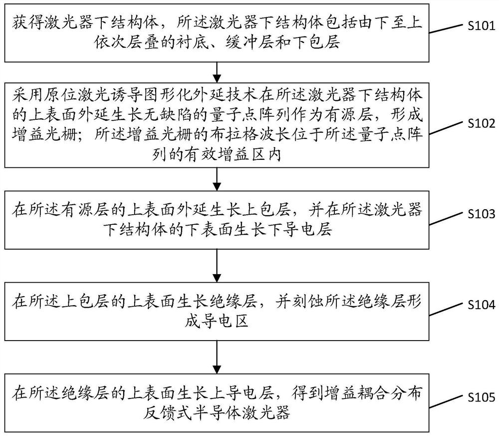
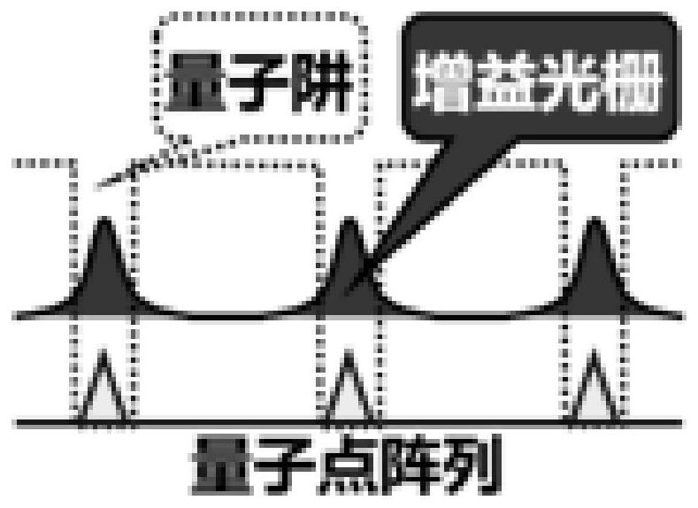
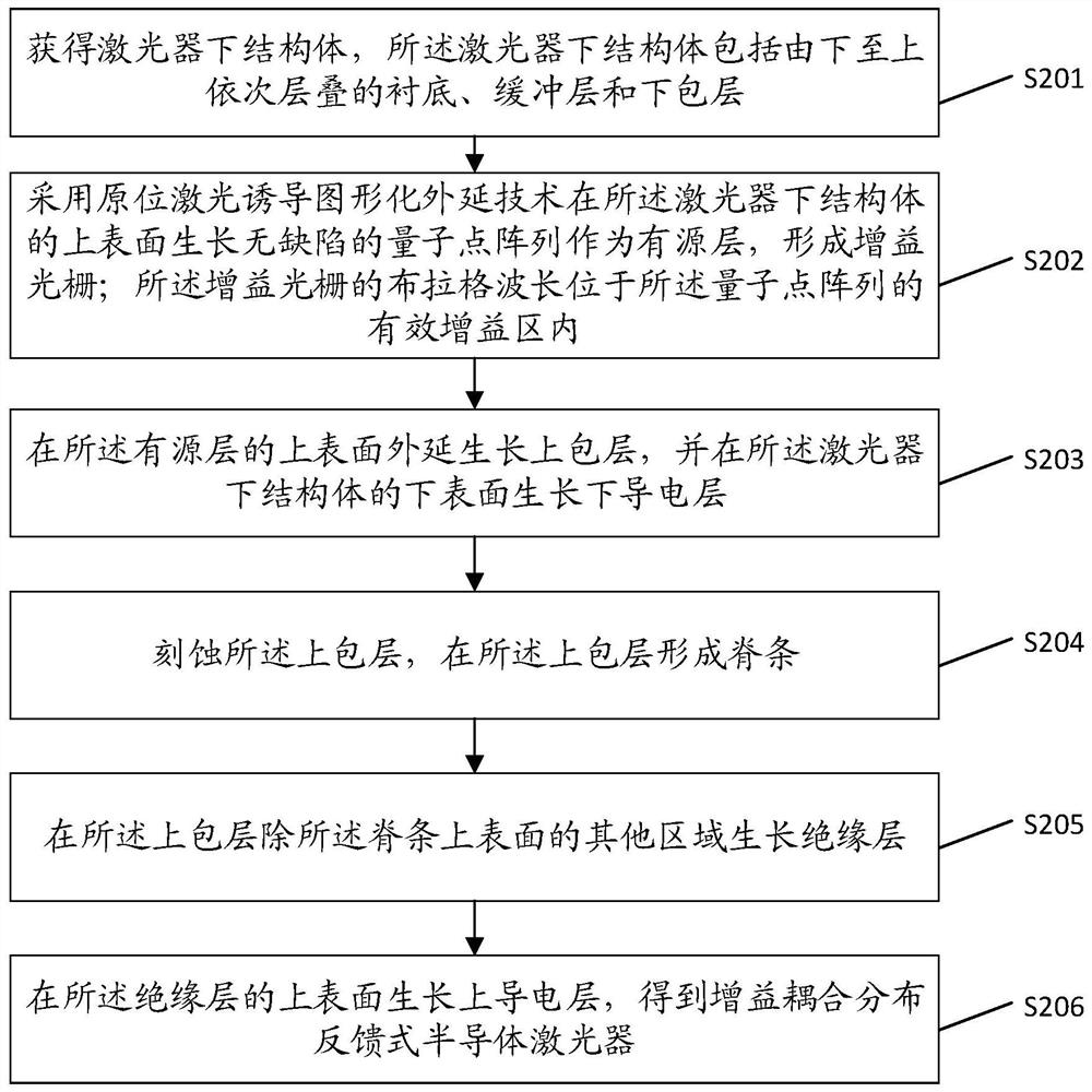
[0044] In order to enable those skilled in the art to better understand the solution of the present application, the present application will be further described in detail below in conjunction with the drawings and specific implementation methods. Apparently, the described embodiments are only some of the embodiments of this application, not all of them. Based on the embodiments in this application, all other embodiments obtained by persons of ordinary skill in the art without making creative efforts belong to the scope of protection of this application.

[0045] In the following description, a lot of specific details are set forth in order to fully understand the present invention, but the present invention can also be implemented in other ways different from those described here, and those skilled in the art can do it without departing from the meaning of the present invention. By analogy, the present invention is therefore not limited to the specific examples disclosed bel...


PUM


Abstract

The invention discloses a gain coupling distributed feedback type semiconductor laser and a manufacturing method thereof. The method comprises the steps of: obtaining a laser lower structural body which comprises a substrate, a buffer layer and a lower cladding which are sequentially stacked from bottom to top; epitaxially growing a defect-free quantum dot array as an active layer on the upper surface of the laser lower structural body by adopting an in-situ laser-induced graphical epitaxy technology to form a gain grating of which the Bragg wavelength is located in an effective gain region of the quantum dot array; epitaxially growing an upper cladding on the upper surface of the active layer, and growing a lower conductive layer on the lower surface of the laser lower structural body; growing an insulating layer on the upper surface of the upper cladding, and etching the insulating layer to form a conductive region; and growing an upper conductive layer on the upper surface of the insulating layer to obtain the gain coupling distributed feedback type semiconductor laser. The active layer is grown by adopting an in-situ laser-induced graphical epitaxy technology, so that defects can be prevented from being introduced. No grating needs to be prepared, pure gain coupling is achieved, and the manufacturing process is very simple.

Description

technical field [0001] The present application relates to the field of semiconductor technology, in particular to a gain-coupling distributed feedback semiconductor laser and a manufacturing method thereof. Background technique [0002] Semiconductor lasers are called semiconductor laser diodes, or laser diodes (Laser Diode, LD), which have the advantages of small size, light weight, low power drive, high efficiency output, convenient modulation, long life and easy integration. Semiconductor lasers can be divided into ordinary Fabry-Perot (Fabry-Perot, FP for short) lasers and distributed feedback (Distributed Feed Back, DFB for short) lasers. Among them, the manufacturing process of FP-LD is simple, and the production of DFB-LD The process is complex. [0003] The gain-coupled distributed feedback semiconductor laser is a kind of DFB-LD. There are three main ways to prepare the traditional gain-coupled distributed feedback semiconductor laser. The first is to directly etch...

Claims


Application Information

Patent Timeline
Patent Type & Authority Applications(China)
IPC IPC(8): H01S5/12
CPCH01S5/1228H01S5/1231
Inventor 彭长四石震武耿彪杨新宁缪力力庄思怡祁秋月
Owner SUZHOU UNIV
Why Eureka
Try Eureka