Organic Light Emitting Device and Manufacturing Method Thereof

a light emitting device and organic technology, applied in the direction of solid-state devices, electric lighting sources, electric light sources, etc., can solve problems such as open edge defects, and achieve the effect of preventing transfer defects and improving pattern image characteristics

Inactive Publication Date: 2013-06-06
SAMSUNG DISPLAY CO LTD
View PDF6 Cites 5 Cited by
  • Summary
  • Abstract
  • Description
  • Claims
  • Application Information

AI Technical Summary

Benefits of technology

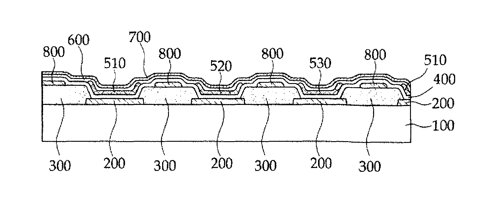
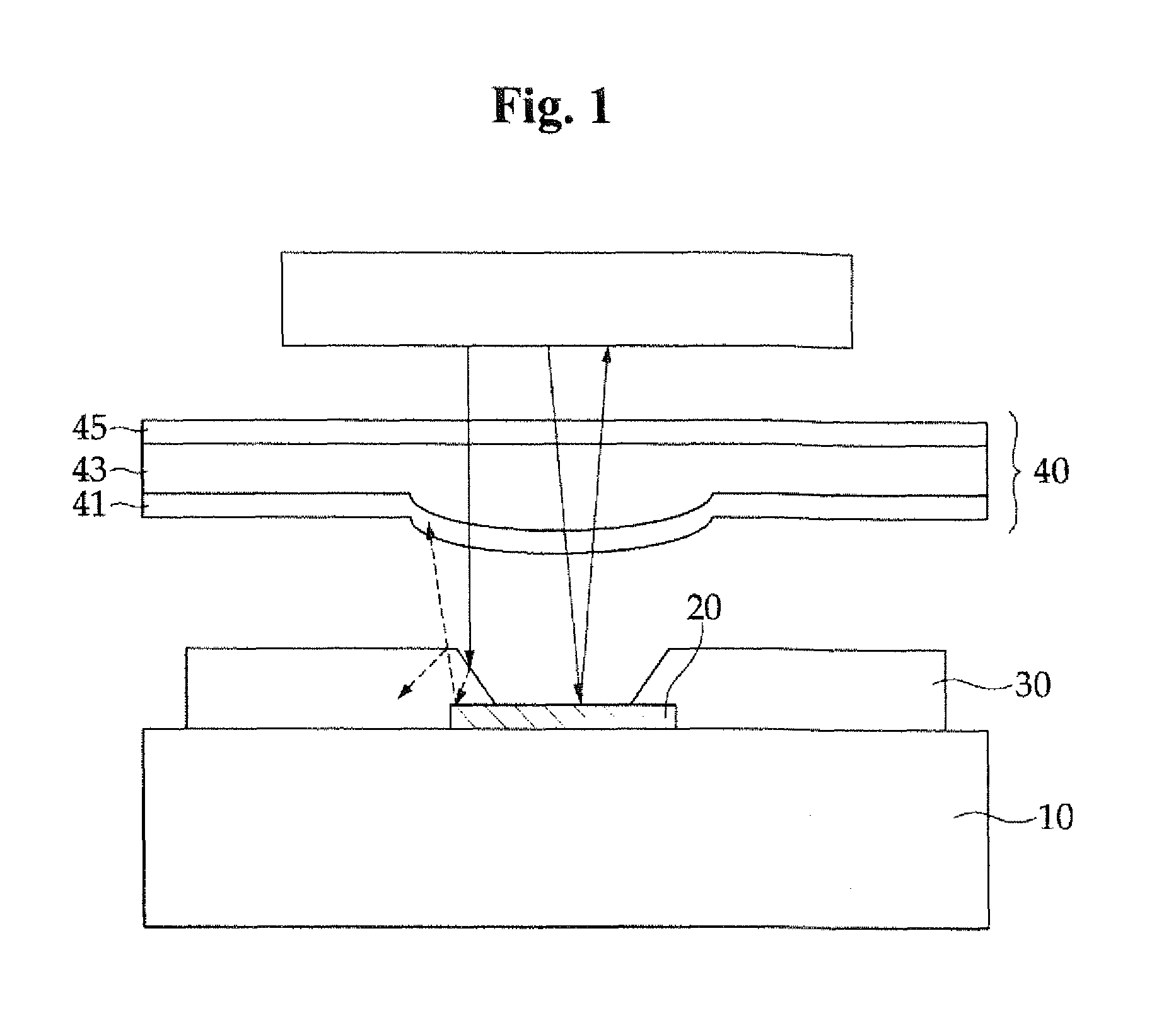
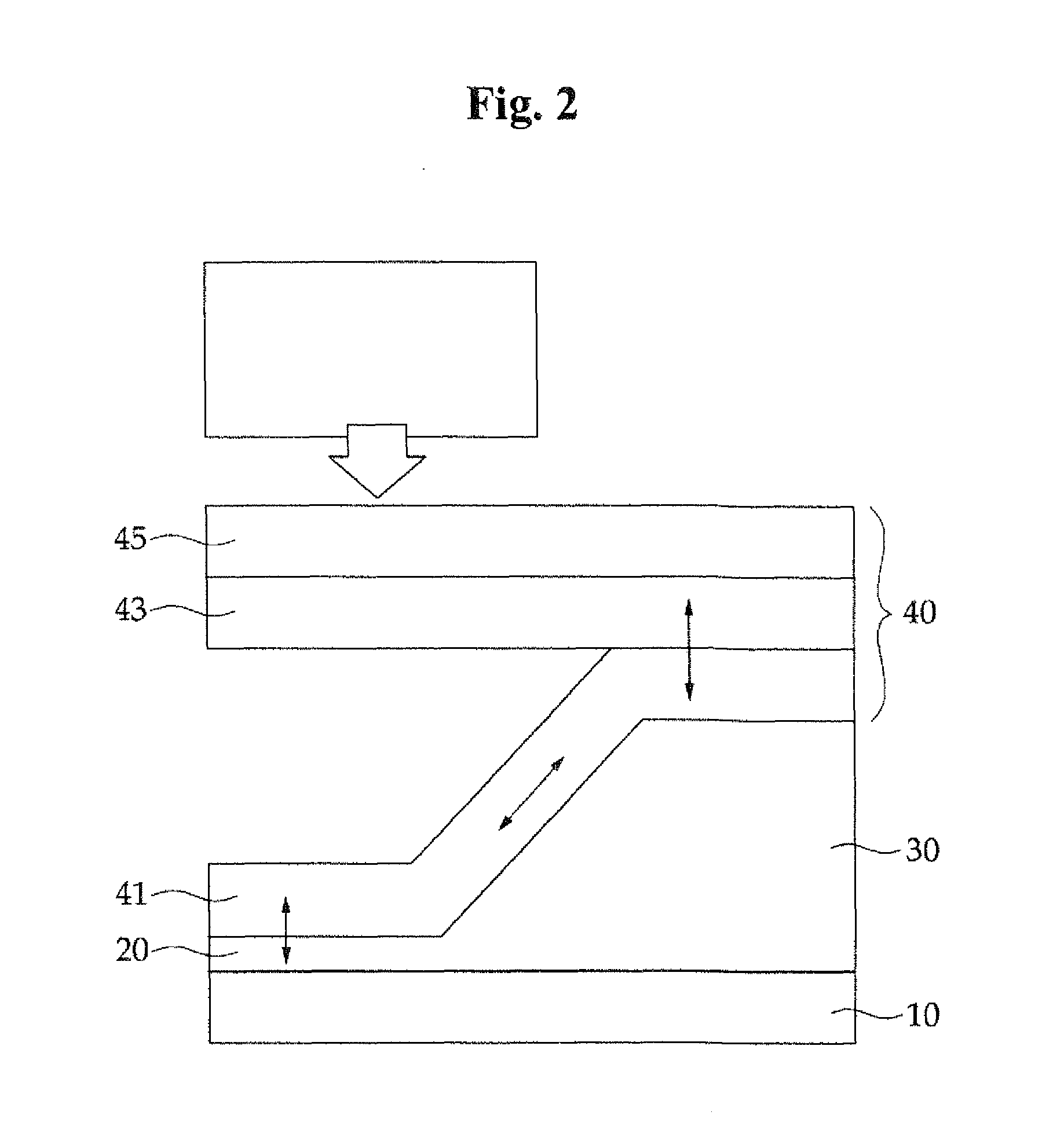
[0034]Accordingly, in the organic light emitting device according to the present invention, the reflective layers are formed in the pixel definition layers, and it is possible to prevent the transfer defect, such as the non-transfer of the edge portion of the electrode, when the transfer is performed through laser irradiation, thereby advantageously improving a pattern image characteristic at the edge portion of the electrode.
[0035]Furthermore, according to the method of manufacturing the organic light emitting device of the present invention, the step of forming the first electrodes and the step of forming the reflective layers are simultaneously performed, so that it is possible to manufacture an organic light emitting device in which the non-transfer defect is prevented without an additional mask or adding a complicated process.

Problems solved by technology

However, when a transfer is performed through an irradiation of the laser in a state in which a donor film is aligned with a pixel part, an open edge defect may be generated, in which a portion in an edge part may not be transferred due to a continuous application of a forte between a portion that has been irradiated by the laser and a portion that has not been irradiated by the laser.

Method used


Image

  • Organic Light Emitting Device and Manufacturing Method Thereof
  • Organic Light Emitting Device and Manufacturing Method Thereof
  • Organic Light Emitting Device and Manufacturing Method Thereof

Examples


Embodiment Construction

[0044]Hereinafter, exemplary embodiments of the present invention will be described with reference to the accompanying drawings. However, it should be noted that the scope of the present invention is not limited by the below-described embodiments and the drawings. Furthermore, it will be understood that all changes, equivalents, or substitutes included in the spirit and technical scope of the present invention are included in the scope of the present invention.

[0045]Although terms used herein are selected from widely used general terms as often as possible, several terms were selected by the applicant of the present invention depending on particular circumstances, and in this case the meaning of the terms selected by the applicant should be understood considering a meaning described or used in the detailed description of the present invention.

[0046]For reference, a part irrelevant to the description will be omitted for clarity of the present invention. In the following description, ...


PUM


Abstract

In an organic light emitting device and a method of manufacturing the organic light emitting device, reflective layers are formed on pixel definition layers to prevent the generation of an open edge defect (or a non-transfer defect) in forming light emitting layers. The organic light emitting device includes a base, first electrodes patterned and formed on the base, light emitting layers formed on the first electrodes, and a second electrode formed on the light emitting layers. Pixel definition layers are formed between the patterned first electrodes, and reflective layers are disposed in the pixel definition layers.

Description

CLAIM OF PRIORITY[0001]This application makes reference to, incorporates the same herein, and claims all benefits accruing under 35 U.S.C. §119 from an application for ORGANIC LIGHT EMITTING DEVICE AND MANUFACTURING METHOD THEREOF earlier filed in the Korean Intellectual Property Office on 6 Dec. 2011 and there duly assigned Serial No. 10-2011-0129388.BACKGROUND OF THE INVENTION[0002]1. Field of the Invention[0003]The present invention relates to an organic light emitting device and a method of manufacturing the organic light emitting device, and more particularly to an organic light emitting device and a method of manufacturing the organic light emitting device, in which reflective layers are formed on pixel definition layers, thereby preventing the generation of a non-transfer defect during formation of light emitting layers.[0004]2. Description of the Related Art[0005]In recent years, organic light emitting devices are being spotlighted in the field of display technology. Such an...

Claims


Application Information

Patent Timeline
Patent Type & Authority Applications(United States)
IPC IPC(8): H01L51/50H01L51/56
CPCH01L27/3283H01L51/0013H10K59/173H10K71/18H05B33/24H10K50/856
Inventor KIM, NAM-JINPARK, CHUL-HWAN
Owner SAMSUNG DISPLAY CO LTD
Why Eureka
Try Eureka