Crystalline silicon-based solar cell

a solar cell and crystalline silicon technology, applied in the direction of sustainable manufacturing/processing, climate sustainability, semiconductor devices, etc., can solve the problems of increasing costs, increasing electrical junctions, and improving the efficiency of carrier extraction, so as to achieve excellent photoelectric conversion efficiency and high carrier density

Inactive Publication Date: 2013-06-13
KANEKA CORP
View PDF6 Cites 14 Cited by
  • Summary
  • Abstract
  • Description
  • Claims
  • Application Information

AI Technical Summary

Benefits of technology

[0018]In a crystalline silicon-based solar cell of the present invention, a first transparent electrode layer is composed of two or more layers, and a substrate-side electroconductive layer in contact with a crystalline silicon-based thin-film has a relatively high carrier density. Thus, an electrical junction between the silicon-based thin-film and the transparent electrode layer is improved

Problems solved by technology

However, indium oxide doped with tungsten as in Patent Document 2 may cause an increase in costs, for example, due to a necessity of adding zinc in a slight amount as a coagulant in a step for producing a target used for deposition.
In the heterojunction-type solar cell, the transparent electrode layer is important in extraction of photoinduced carriers, but improvement of carrier extraction efficiency cannot be expected merely by making the transparent e

Method used


Image

  • Crystalline silicon-based solar cell
  • Crystalline silicon-based solar cell
  • Crystalline silicon-based solar cell

Examples


example 1

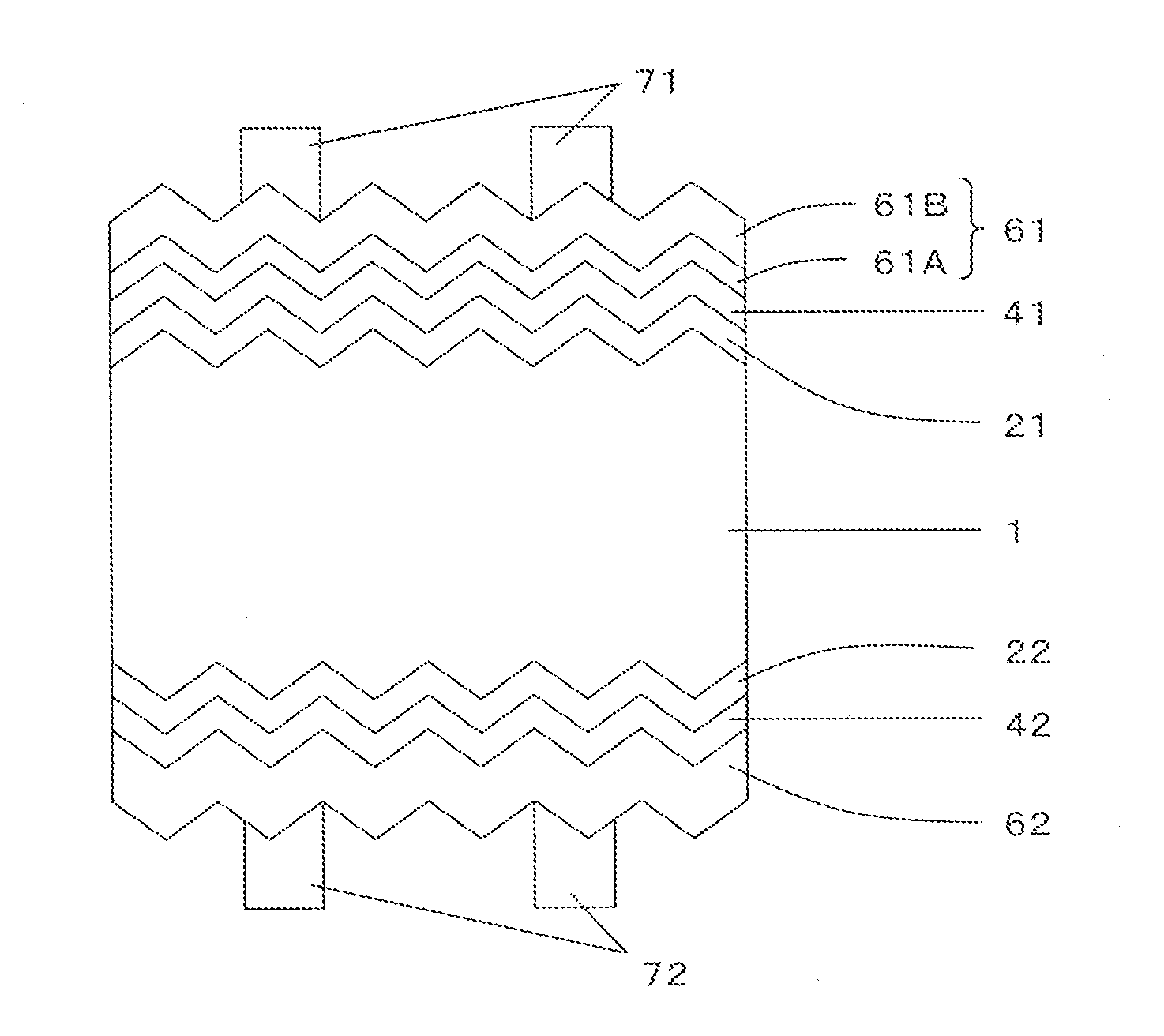
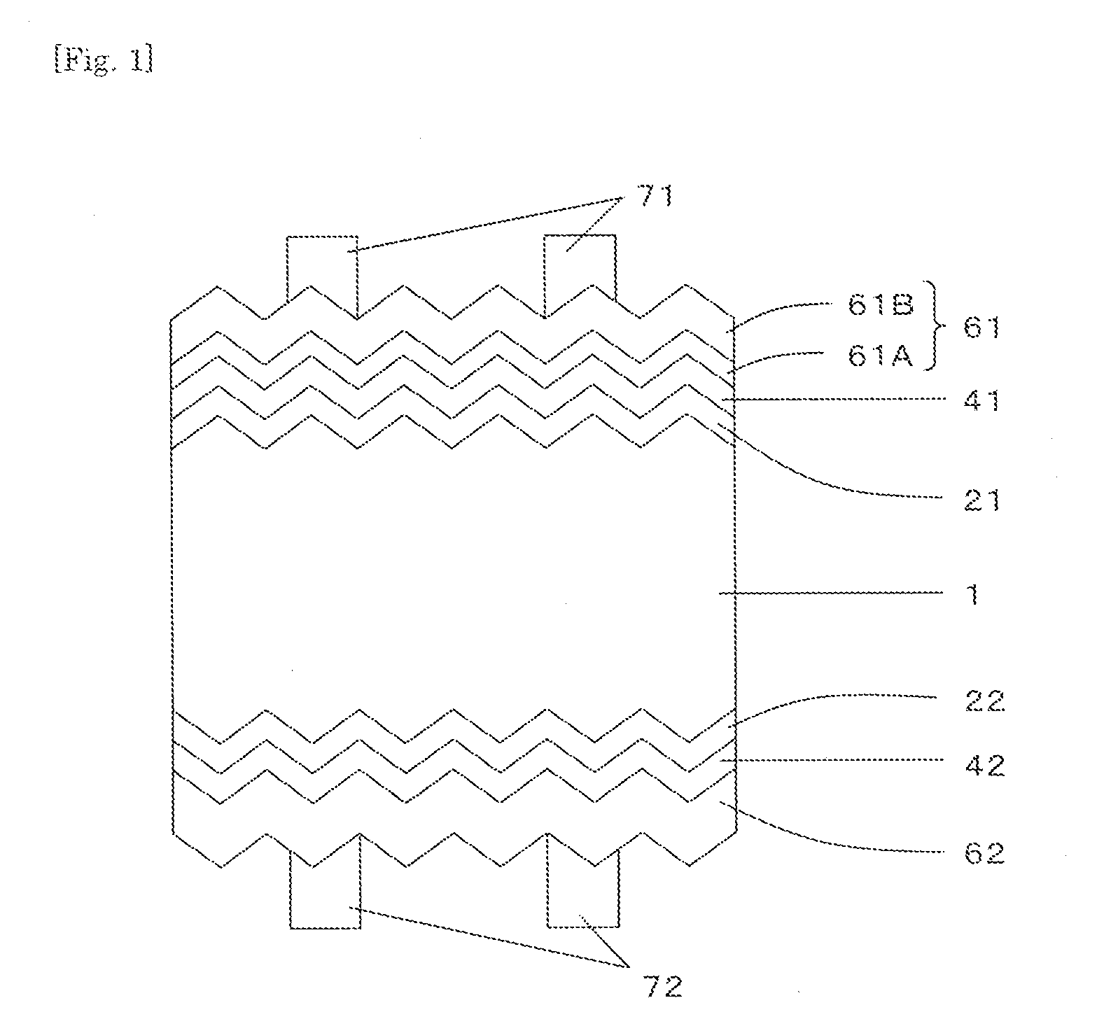
[0083]A crystalline silicon-based solar cell schematically shown in FIG. 1 was prepared. The crystalline silicon-based solar cell of this Example is a heterojunction solar cell, wherein both surfaces of an n-type single-crystal silicon substrate 1 are textured surfaces. On the light incident side of the n-type single-crystal silicon substrate 1, a first intrinsic amorphous silicon layer 21, a p-type amorphous silicon layer 41, a first transparent electrode layer 61 and a collecting electrode 71 are formed in this order. The first transparent electrode layer has a two-layer structure in which a surface-side electroconductive layer 61B is formed on a substrate-side electroconductive layer 61A. On the back surface-side of the n-type single-crystal silicon substrate 1, a second intrinsic amorphous silicon layer 22, an n-type amorphous silicon layer 42, a second transparent electrode layer 62 and a collecting electrode 72 are formed in this order. This crystalline silicon-based solar cel...


PUM


Abstract

The present invention improves a photoelectric conversion efficiency of a crystalline silicon-based solar cell. The crystalline silicon based solar cell includes a silicon-based thin-film of a first conductivity type and a first transparent electrode layer, in this order, on one surface of a conductive single-crystal silicon substrate, and a silicon-based thin-film of the opposite conductivity type and a second transparent electrode layer, in this order, on the other surface of the conductive single-crystal silicon substrate. The first and second transparent electrode layers are each formed of a transparent conductive metal oxide, and the first transparent electrode layer preferably has at least two layers, and a total thickness of 50 to 120 nm, wherein the carrier density of the substrate-side electroconductive layer is higher than that of the surface-side electroconductive layer, and the carrier density of the surface-side electroconductive layer is 1 to 4×1020 cm−3.

Description

TECHNICAL FIELD[0001]The invention relates to a crystalline silicon-based solar cell having a heterojunction on a surface of a single-crystal silicon substrate.BACKGROUND ART[0002]Crystalline silicon-based solar cells using crystalline silicon substrates are high in photoelectric conversion efficiency, and thus have already been widely and generally used in solar power generation systems. Among solar cells, a particular crystalline silicon-based solar cell in which an amorphous silicon-based thin-film having a band gap different from that of a single-crystal silicon is formed on a surface of the crystalline silicon substrate to produce a diffusion potential is called a heterojunction solar cell.[0003]Among heterojunction-type solar cells, a solar cell having an intrinsic amorphous silicon thin-film between a conductive amorphous silicon-based thin-film for forming a diffusion potential and a single-crystal silicon substrate is known as one embodiment of a crystalline silicon-based s...

Claims


Application Information

Patent Timeline
IPC IPC(8): H01L31/0224
CPCH01L31/022466H01L31/022475Y02E10/50H01L31/202H01L31/0747Y02P70/50
Inventor KUCHIYAMA, TAKASHIYAMAMOTO, KENJIYOSHIMI, MASASHI
Owner KANEKA CORP
Why Eureka
Try Eureka