

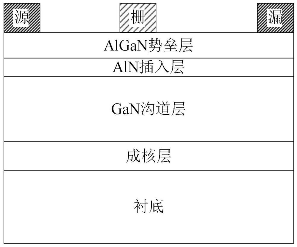
YAlN/GaN high-electron-mobility transistor and manufacturing method thereof
A high electron mobility, transistor technology, applied in semiconductor/solid-state device manufacturing, circuits, electrical components, etc., can solve the high-density dislocation defects of heterogeneous epitaxial GaN materials, shorten the length of the device gate, increase the operating frequency, and affect the device Problems such as current and power output characteristics, to achieve the effect of improving device current and power output characteristics, improving device current and power characteristics, and increasing carrier concentration
- Summary
- Abstract
- Description
- Claims
- Application Information
AI Technical Summary
Problems solved by technology
Method used
Image

Examples
Embodiment 1
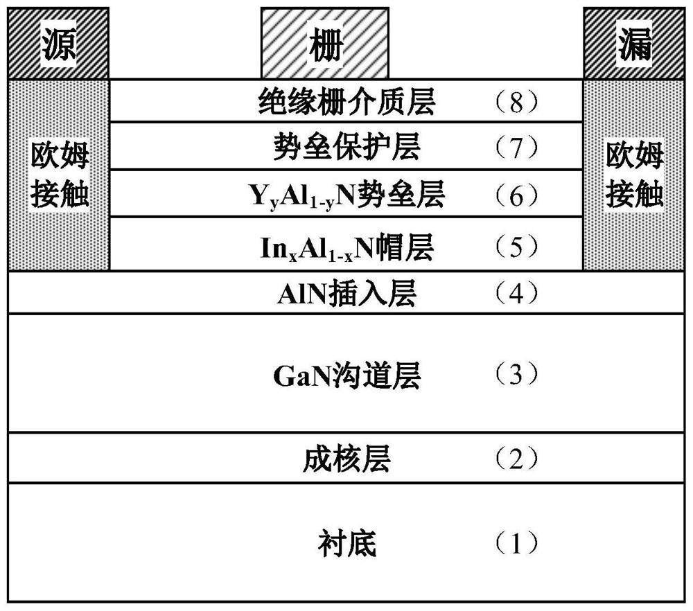
[0054] Embodiment one, the production adopts In 0.14 Al 0.86 N cap layer, Y 0.06 Al 0.94 Sapphire-based YAlN / GaN high electron mobility transistor with N barrier layer.
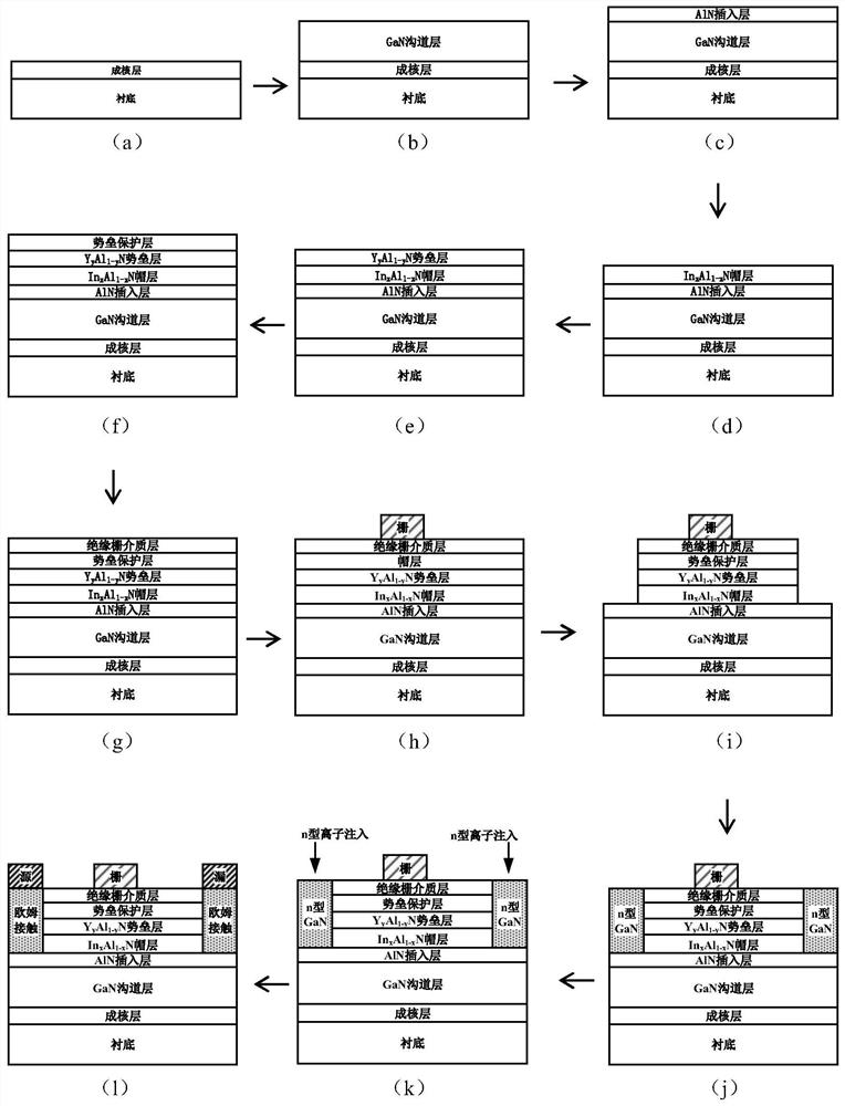
[0055] Step 1, epitaxial AlN nucleation layer, such as image 3 (a).
[0056] A metal-organic chemical vapor deposition technique was used to epitaxially form an AlN nucleation layer with a thickness of 100 nm on a sapphire substrate.
[0057] The process conditions adopted for the epitaxial AlN nucleation layer are as follows: temperature is 1200° C., pressure is 40 Torr, ammonia gas flow is 2000 sccm, aluminum source flow is 20 sccm, and hydrogen gas flow is 3000 sccm.
[0058] Step 2, depositing a GaN channel layer, such as image 3 (b).
[0059] A GaN channel layer with a thickness of 3000 nm was deposited on the AlN nucleation layer using metal organic chemical vapor deposition technique.
[0060] The process conditions for depositing the GaN channel layer are: temperature 1080°C, pressure 40 Tor...
Embodiment 2
[0086] Embodiment two, the production adopts In 0.2 Al 0.8 N cap layer, Y 0.15 Al 0.85 Si-based YAlN / GaN high electron mobility transistor with N barrier layer.
[0087] Step 1, epitaxial AlN and AlGaN and AlGaN / GaN superlattice composite nucleation layer using metal-organic chemical vapor deposition technology, such as image 3 (a).
[0088] (1a) under the process conditions that the temperature is 1100° C., the pressure is 40 Torr, the flow rate of ammonia gas is 2000 sccm, the flow rate of aluminum source is 20 sccm, and the flow rate of hydrogen gas is 3000 sccm, an AlN nucleation layer with a thickness of 60 nm is epitaxially formed on the Si substrate;
[0089](1b) The temperature is 1100°C, the pressure is 40 Torr, the ammonia gas flow rate is 2000 sccm, the aluminum source flow rate is 20 sccm, the gallium source flow rate is 120 sccm, and the hydrogen gas flow rate is 3000 sccm, and the deposition thickness on the AlN nucleation layer is 80nm AlGaN nucleation lay...
Embodiment 3
[0112] Embodiment three, the production adopts In 0.17 Al 0.83 N cap layer, Y 0.11 Al 0.89 SiC-based YAlN / GaN high electron mobility transistor with N barrier layer.
[0113] Step A, epitaxial AlN nucleation layer, such as image 3 (a).
[0114] Using the metal-organic chemical vapor deposition technology, set the temperature at 1150°C, the pressure at 40Torr, the flow rate of ammonia gas at 2000sccm, the flow rate of aluminum source at 30sccm, and the flow rate of hydrogen gas at 3000sccm, and deposit a thickness of 120nm on the SiC substrate. High temperature AlN nucleation layer.
[0115] Step B, deposit GaN channel layer, such as image 3 (b).
[0116] Using metal-organic chemical vapor deposition technology, under the process conditions of temperature 1150°C, pressure 40Torr, ammonia gas flow rate 2000 sccm, gallium source flow rate 100 sccm, hydrogen gas flow rate 3000 sccm, the thickness of the AlN nucleation layer is deposited as follows: 1500nm GaN channel lay...
PUM
| Property | Measurement | Unit |
|---|---|---|
| thickness | aaaaa | aaaaa |
| thickness | aaaaa | aaaaa |
| thickness | aaaaa | aaaaa |
Abstract
Description
Claims
Application Information