Liquid crystal display device and touch panel

a technology touch panel, which is applied in the direction of instruments, computing, electric digital data processing, etc., can solve the problems of reducing reliability, unable to use existing equipment in the manufacturing factory of liquid crystal display device, and unable to solve the problem of reducing reliability

Active Publication Date: 2016-06-14
SEMICON ENERGY LAB CO LTD
View PDF194 Cites 7 Cited by
  • Summary
  • Abstract
  • Description
  • Claims
  • Application Information

AI Technical Summary

Benefits of technology

[0019]It is found from our research that entry of water into an oxide semiconductor film is one of big facts of a change in electric characteristics of an oxide semiconductor transistor. Entry of water into the oxide semiconductor film increases carrier density, so that electric characteristics of the transistor are varied.
[0025]According to the technique disclosed in this specification, a liquid crystal display device having as high reliability as a practical level, whose backplane is formed using an oxide semiconductor, can be provided.

Problems solved by technology

For that reason, a liquid crystal display device is manufactured using a material containing water as little as possible and by a structure and a manufacturing method which prevents entry of water as much as possible, which leads to resolution of decrease in reliability.
However, limitation of a material causes new problems in that display quality of a liquid crystal display device is decreased and that existing equipment in a manufacturing factory of liquid crystal display devices cannot be used; thus, early practical application of liquid crystal display devices including an oxide semiconductor is hindered.
However, an organic resin film has a higher hygroscopic property than an inorganic insulating film; thus, there is a problem in combination with an oxide semiconductor transistor.

Method used


Image

  • Liquid crystal display device and touch panel
  • Liquid crystal display device and touch panel
  • Liquid crystal display device and touch panel

Examples


embodiment 1

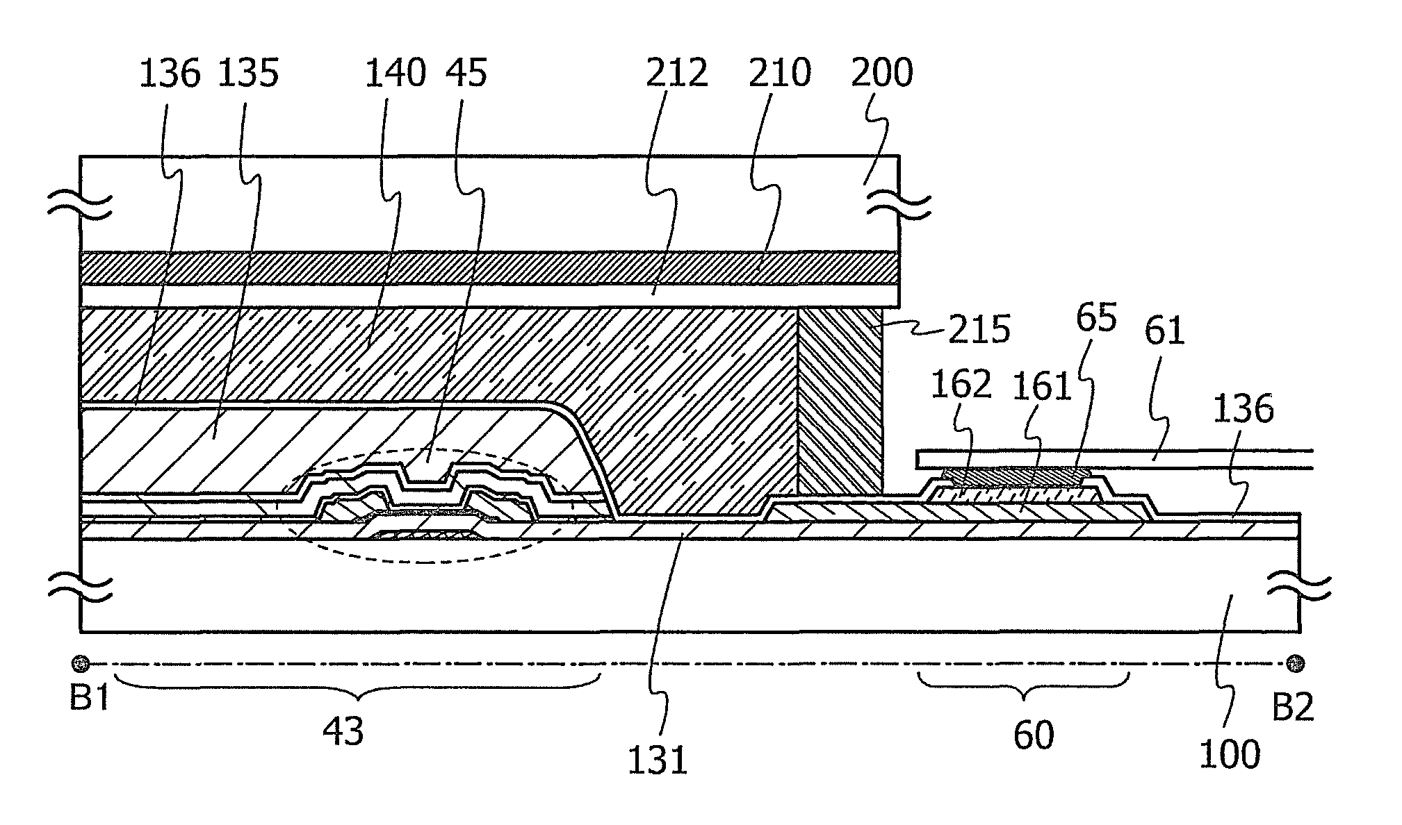
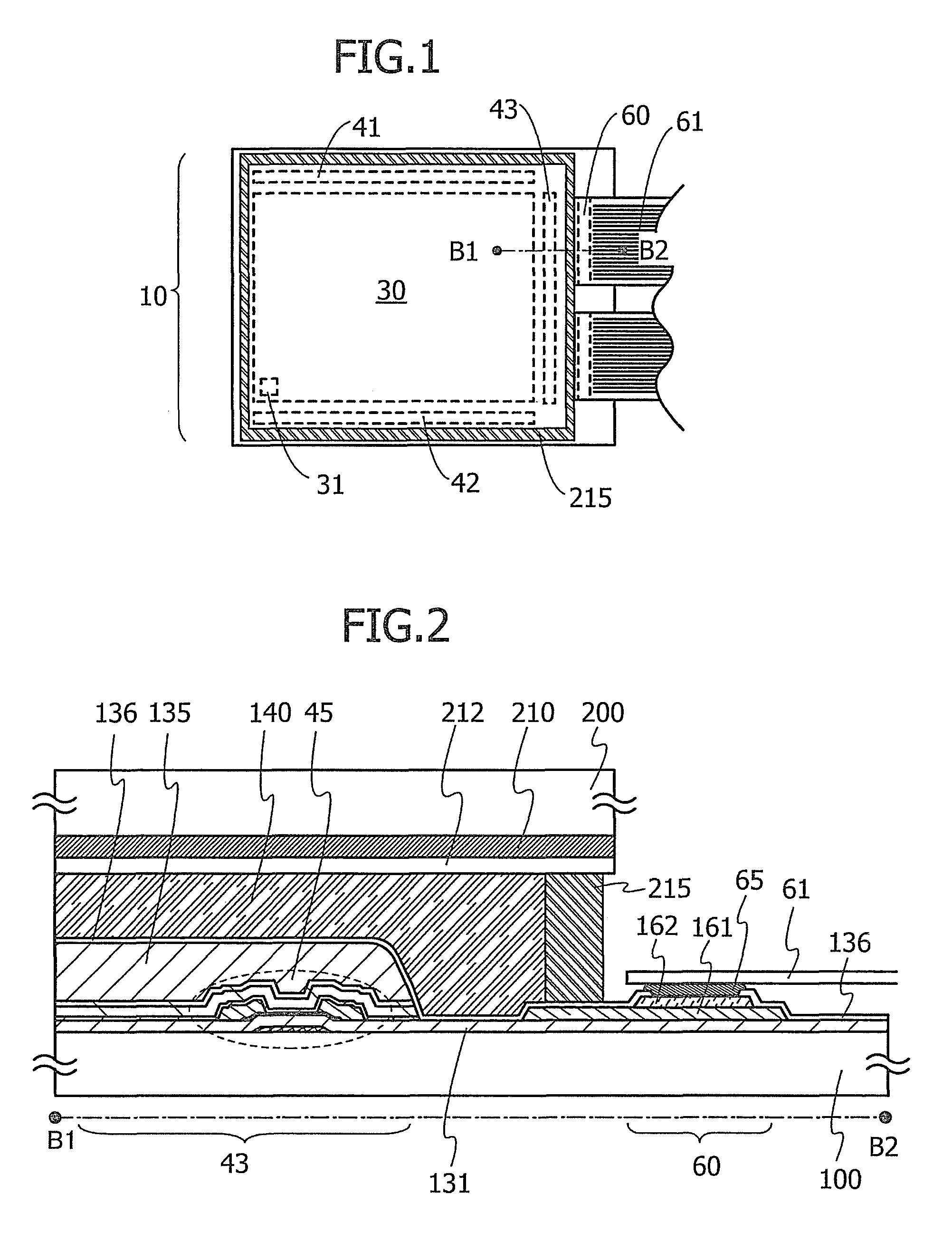
[0054]A liquid crystal panel of one embodiment of the present invention is described with reference to FIG. 1 to FIG. 6 and FIGS. 10A and 10B.

[0055]FIG. 10A is a block diagram illustrating a structural example of a liquid crystal panel 10. The liquid crystal panel 10 includes a display portion 30, a scan line driver circuit 41, a scan line driver circuit 42, and a data line driver circuit 43. In the liquid crystal panel 10, the driver circuits 41 to 43 and the display portion 30 are formed over the same substrate, a board 100; thus, the liquid crystal panel 10 is also referred to as a liquid crystal module. The liquid crystal panel 10, a control circuit thereof, a power supply circuit, a back light module, and the like are incorporated in a housing, so that a liquid crystal display device is completed.

[0056]The display portion 30 includes a plurality of pixels 31 each of which is connected to a scan line 110 and a data line 111. FIG. 10B is a circuit diagram showing a structural exa...

embodiment 2

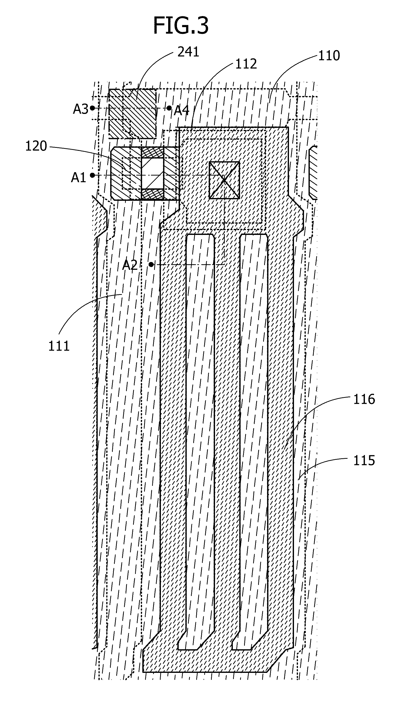
[0145]In this embodiment, a transistor included in the pixel 31 and the driver circuits 41 to 43 of the liquid crystal panel 10 is described.

120>

[0146]As the oxide semiconductor used for the semiconductor layer 120 of a transistor, for example, any of the following can be used: indium oxide, tin oxide, zinc oxide, an In—Zn-based oxide, a Sn—Zn-based oxide, an Al—Zn-based oxide, a Zn—Mg-based oxide, a Sn—Mg-based oxide, an In—Mg-based oxide, an In—Ga-based oxide, an In—Ga—Zn-based oxide (also referred to as IGZO), an In—Al—Zn-based oxide, an In—Sn—Zn-based oxide, a Sn—Ga—Zn-based oxide, an Al—Ga—Zn-based oxide, a Sn—Al—Zn-based oxide, an In—Hf—Zn-based oxide, an In—Zr—Zn-based oxide, an In—Ti—Zn-based oxide, an In—Sc—Zn-based oxide, an In—Y—Zn-based oxide, an In—La—Zn-based oxide, an In—Ce—Zn-based oxide, an In—Pr—Zn-based oxide, an In—Nd—Zn-based oxide, an In—Sm—Zn-based oxide, an In—Eu—Zn-based oxide, an In—Gd—Zn-based oxide, an In—Tb—Zn-based oxide, an In—Dy—Zn-based oxide, an In—...

embodiment 3

[0196]The liquid crystal panel 10 in FIG. 1 provided with a touch sensor (contact detector) can function as a touch panel.

[0197]In this embodiment, a touch panel is described with reference to FIG. 12, FIG. 13, and FIGS. 14A and 14B.

[0198]FIG. 12 is a cross-sectional view illustrating a structural example of a touch panel 400 using the liquid crystal panel 10. FIG. 13 is a plan view illustrating a structural example of the common electrode 421 and the electrode 422 of the touch panel 400. FIG. 14A is a cross-sectional view taken along line C1-C2 in FIG. 13, and FIG. 14B is a plan view of a region 240 in FIG. 13.

[0199]The touch panel 400 includes a capacitive sensor as a touch sensor. A polarizing plate 411 is attached to the outer side of the substrate 100, and a polarizing plate 412 is attached to the outer side of the substrate 200.

[0200]A common electrode 421 over the substrate 100 serves as a common electrode of a pixel and an electrode of a capacitor in the touch sensor. The el...


PUM

PropertyMeasurementUnit
temperatureaaaaaaaaaa
dew pointaaaaaaaaaa
capacitanceaaaaaaaaaa

Abstract

A semiconductor layer of a transistor is formed of an oxide semiconductor film including a crystal part. An organic resin film covering the transistor is formed. By treatment such as drying treatment on the organic resin film in a cell process, variations in the threshold voltage of the oxide semiconductor transistor due to moisture can be suppressed. A common electrode faces a pixel electrode. The common electrode and the pixel electrode are formed over the organic resin film with an insulating film provided therebetween. Therefore, a capacitor can be provided to a liquid crystal element if a pixel does not include a wiring for a storage capacitor. An antistatic electrode is provided on the outer side of a color filter substrate and the capacitance between the antistatic electrode and the common electrode is utilized, so that the liquid crystal display device can be used as a touch panel.

Description

BACKGROUND OF THE INVENTION[0001]1. Field of the Invention[0002]The present invention relates to a liquid crystal display device including a transistor using an oxide semiconductor and a touch panel including the liquid crystal display device.[0003]2. Description of the Related Art[0004]Transistors which are used for many liquid crystal display devices and organic EL display devices have been formed using a silicon semiconductor film such as an amorphous silicon film or a polycrystalline silicon film.[0005]Instead of the silicon semiconductor film, a technique in which an oxide semiconductor film is used for transistors has attracted attention.[0006]For example, a technique is disclosed in which a transistor manufactured using an In—Ga—Zn oxide film as an oxide semiconductor is used as a switching element or the like of a pixel (see Patent Documents 1 and 2).[0007]Further, we develop a technique in which an oxide semiconductor film having a noble crystal structure is manufactured ov...

Claims


Application Information

Patent Timeline
Patent Type & Authority Patents(United States)
IPC IPC(8): G02F1/1333G06F3/041G06F3/044G02F1/1341
CPCG02F1/13338G02F1/1341G06F3/0412G06F3/044G02F2001/13415G06F3/0445G06F3/0446G02F1/13415
Inventor YAMAZAKI, SHUNPEIHIRAKATA, YOSHIHARUKUBOTA, DAISUKEYAMASHITA, AKIO
Owner SEMICON ENERGY LAB CO LTD
Why Eureka
Try Eureka