Ultraviolet-transparent conductive film and process for producing the same

a technology ultraviolet light, applied in the direction of conductive layer on insulating support, non-metal conductor, semiconductor/solid-state device details, etc., can solve the problems of not being provided any report of verifying transparent conductivity in thin-film form, not being able to describe transparency nor applicability of transparent conductive film, and preventing electrostatic charge in the surface

Inactive Publication Date: 2005-05-24
HOYA CORP +1
View PDF6 Cites 9 Cited by
  • Summary
  • Abstract
  • Description
  • Claims
  • Application Information

AI Technical Summary

Benefits of technology

[0020]As mentioned above, the applicability of Ga2O3 or ZnGa2O4 to transparent conductive materials has been verified based on single-crystal and polycrystal samples, but it has not been achieved to prepare them as a thin-film and provide an effective transparent conductivity in the thin film. The inventors have found that a substrate temperature arranged at 600 to 1500° C. during film formation allows oxygen deficiency to be formed in a Ga2O3 crystal or allows Sn ion serving as a dopant to be introduced into a Ga2O3 crystal, which makes it possible to form a thin film having a transparent conductivity.
[0028]While a thin film is usually formed as the β phase, the α phase or high-pressure phase might be formed, for example, by using an appropriate single-crystal substrate and producing a stress in the thin film. As compared to the β phase, the α phase has a shorter distance between the adjacent Ga ions and a higher symmetry in crystal structure. Thus, the α phase can provide an ultraviolet-transparent conductive film having a high electric conductivity without anisotropy.
[0032]The limit of the transparency of a transparent conductive film at the long-wavelength edge generally is determined by plasma absorption due to a carrier introduced into the transparent conductive film, because the plasma absorption (due to the carrier) is caused in the near-infra red region. The wavelength causing the plasma absorption is shifted toward a shorter wavelength as the density of the carrier is increased. Thus, when it is required to have a transparency in a wavelength range of 240 to 800 nm, the carrier density should be controlled so as to prevent the plasma absorption from arising in the wavelength of 800 nm or less. The plasma absorption can be readily measured by a spectrophotometer.
[0033]On the other hand, some device requires only the transparency in the deep / near-ultraviolet region but not in the visible region. For example, if it is required to allow transmission only of a light from a near-ultraviolet-light-emitting device such as GaN or ZnO diodes, a mercury lamp, a deuterium lamp, a third harmonics of YAS laser an XeF excimer laser beam, or a KrF excimer laser beam, a higher-density carrier can be introduced to provide enhanced conductive property, at sacrifice of the transparency in the visible region. In this case, the carrier density may be controlled so as to prevent the plasma absorption from arising in the wavelength of 400 nm or less. That is, the conductivity of an ultraviolet-transparent conductive film having a transparency in a wavelength range of 240 to 400 nm can be enhanced, compared to the film having a transparency in a wavelength range of 240 to 800 nm.
[0037]In an experimental test for measuring the properties of an organic material or testing sample while irradiating it with ultraviolet light, the ultraviolet-transparent conductive film is effective to prevent electrostatic charge in the substrate surface or the like. In processing technologies using an ultraviolet laser, it is advantageous to prevent electrostatic charge in the surface of a material to be processed. In this case, a transparent conductive film allowing transmission of a light of 248 nm wavelength can be applied to a process using a KrF excimer laser beam.

Problems solved by technology

These materials have a bandgap of about 3.2 eV or its equivalent wavelength of about 390 nm, and thereby does not allow transmission of near-ultraviolet light or deep-ultraviolet light having a wavelength shorter than the equivalent wavelength.
However, there has not been provided any report of verifying transparent conductivity in a thin-film form required for applications to transparent electrodes or antistatic films.
Further, this report describes neither transparency nor applicability to transparent conductive films.
However, there is no prior art disclosing a ZnGa2O4 thin-film having transparent conductivity.

Method used


Image

  • Ultraviolet-transparent conductive film and process for producing the same
  • Ultraviolet-transparent conductive film and process for producing the same

Examples


example

[0053]The present invention will be described in detail in conjunction with the following Examples.

Inventive Examples 1 to 3, Comparative Examples 1 to 3

[0054]An YSZ single-crystal substrate was installed in a laser-ablation ultra-high vacuum chamber (St-1200 G made by IRIE KOKEN CO., LTD). Then, the substrate is heated by an IR lamp heater, and oxygen gas having a partial pressure of 0 to 2 Pa was introduced into the chamber. For each of Inventive Examples 1 to 3 and Comparative Examples 1 to 3, a substrate temperature and an oxygen partial pressure are set as shown in Table 1.

[0055]A high-purity Ga2O3 target containing 3 mol % of SnO2 as a dopant was used in each of Inventive Examples 1 to 3 and Comparative Examples 1 to 3. Ga2O3 was deposited on the YSZ single-crystal substrate opposed to the target at a distance of 30 mm by irradiating the target with an ArF excimer laser beam (a laser made by Lambda Physic AG). A resulting film has a thickness of 200 nm.

[0056]Through the measur...

example 4

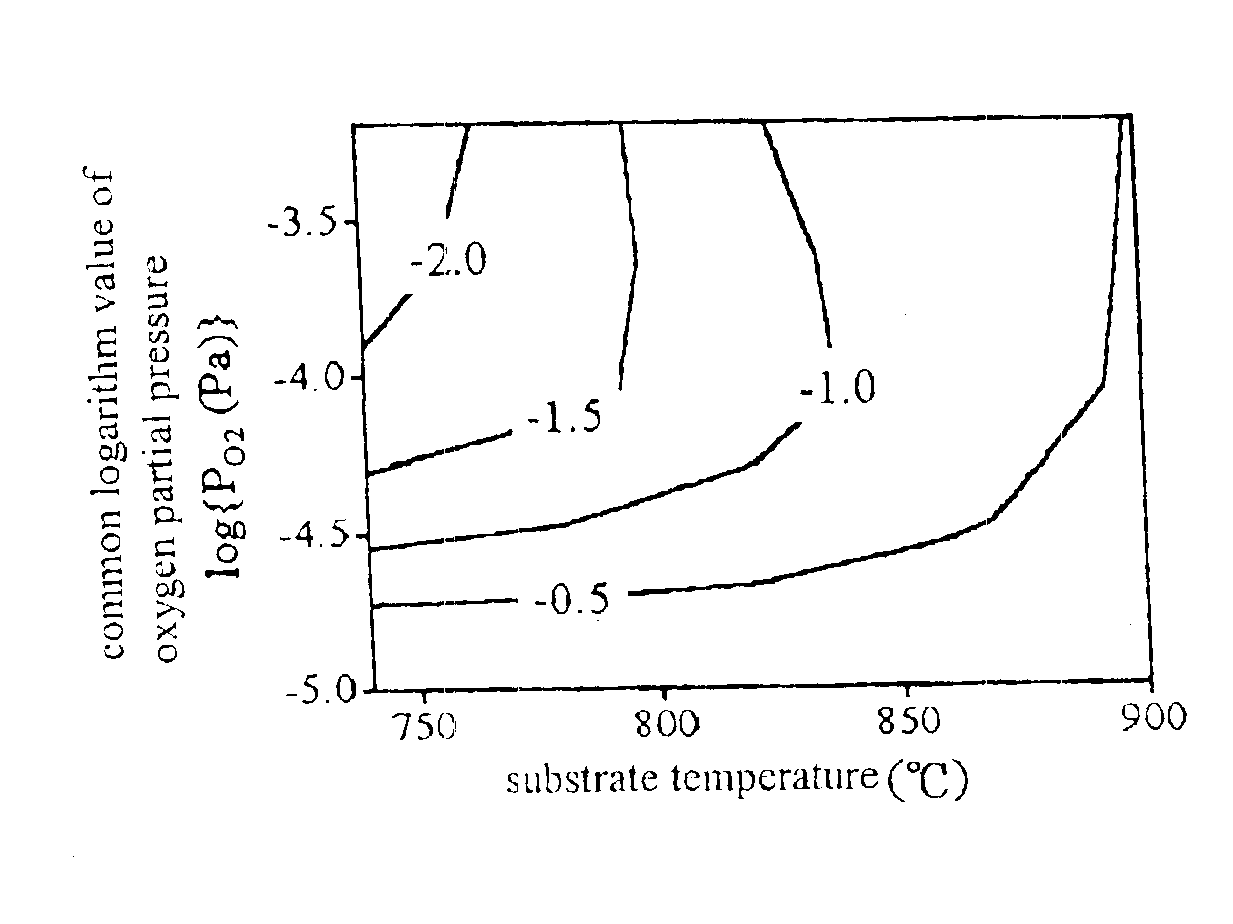
[0058]A silica glass substrate was installed in the laser-ablation ultra-high vacuum chamber. Then, the substrate is heated in the range of 700 to 900° C. by the IR lamp heater, and oxygen gas having a partial pressure in the range of 1×10⁻⁵ to 1×10⁻³ Pa was introduced into the chamber. A high-purity Ga2O3 containing 1 mol % of SnO2 as a dopant was used as a target, and Ga2O3 was deposited on the silica glass substrate opposed to the target at a distance of 30 mm by irradiating the target with the ArF excimer laser beam. A resulting film has a thickness of about 100 nm.

[0059]A conductivity of the thin film with respect to the substrate temperature and oxygen partial pressure is shown in FIG. 1 as a contour diagram. The horizontal axis, vertical axis and contour indicate the substrate temperature, the common logarithm value of the oxygen partial pressure and the common logarithm value of the conductivity, respectively. At a substrate temperature of 750° C., the conductivity is sensit...

example 5

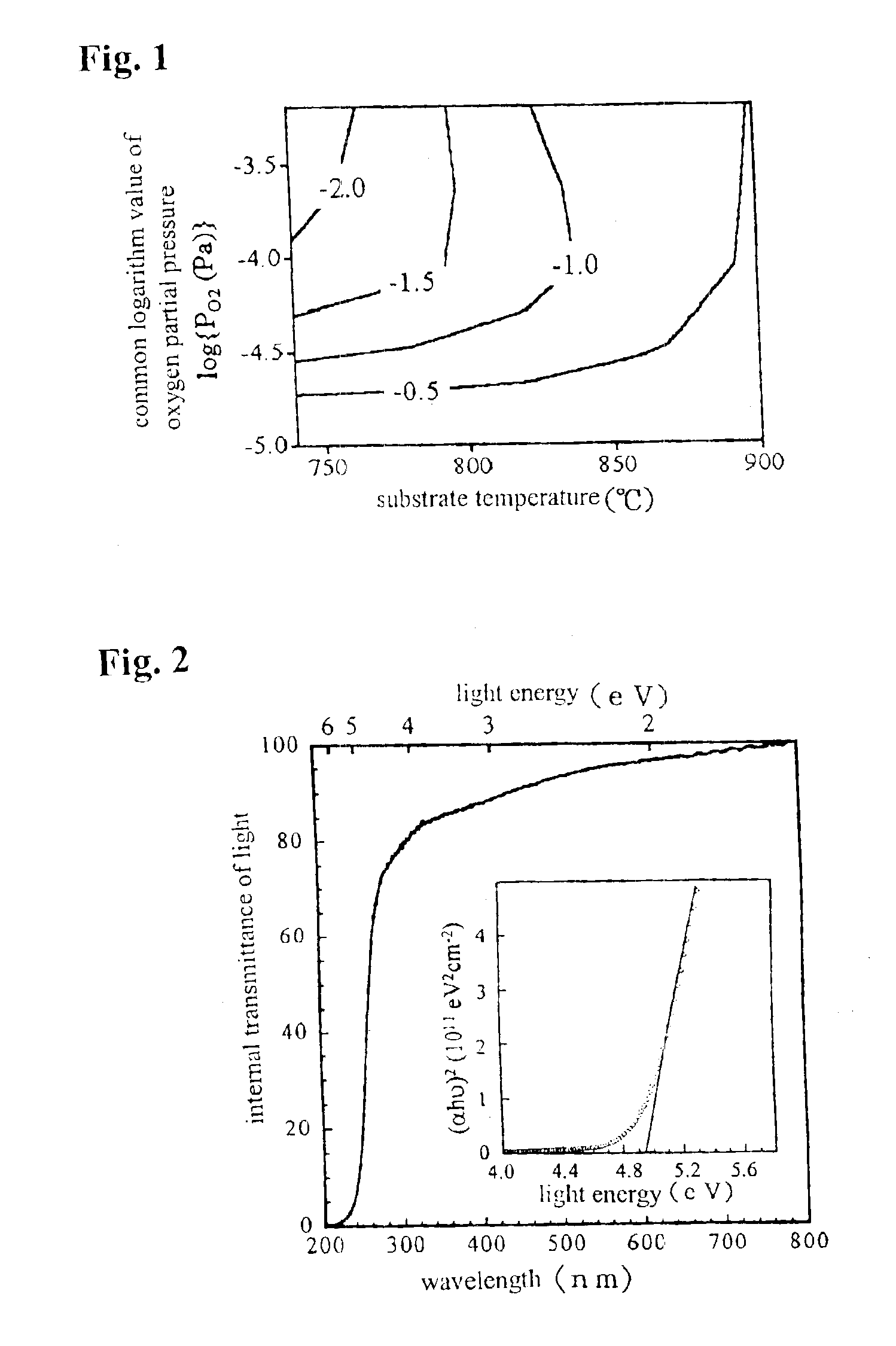
[0060]As in Example 4, Ga2O3 was deposited on a silica glass substrate. Under the conditions with a substrate temperature of 880° C. and an oxygen partial pressure of 6×10⁻⁵ Pa, a β-Ga2O3 thin-film having a conductivity of 1.0 S / cm was obtained. This thin film has a mobility of 0.44 cm2 / Vs and a carrier density of 1.4×10¹⁹ / cm3. A light transmittance spectrum of the thin film is shown in FIG. 2. The horizontal and vertical axes indicate the wavelength of light and the internal transmittance (int) of light, respectively.

[0061]The term “internal transmittance” means a light transmittance in which the contribution of the light reflection on the surface of the thin film is removed therefrom; or a value calculated based on the formula T(int)=T(obs) / (100−R(obs)) using a light transmittance T(obs) and a reflectance R(obs) measured by the ultraviolet / visible spectrophotometer; or a percentage ratio of a transmitted light through the thin film to an original light incident in the thin film.

[0...


PUM

PropertyMeasurementUnit
transmittanceaaaaaaaaaa
light transmittanceaaaaaaaaaa

Abstract

The present invention provides an ultraviolet-transparent conductive film comprising a Ga2O3 crystal. The film has a transparency in the wavelength range of 240 to 800 nm, or 240 to 400 nm, and an electric conductivity induced by an oxygen deficiency or dopant in the Ga2O3 crystal. The dopant includes at least one element selected from the group consisting of the Sn, Ge, Si, Ti, Zr, Hf, V, Nb, Ta, Cr, Mo and W. The ultraviolet-transparent conductive film is formed through either one of a pulsed-laser deposition method, sputtering method, CVD method and MBE method, under the conditions with a substrate temperature of 600 to 1500° C. and an oxygen partial pressure of 0 to 1 Pa.

Description

TECHNICAL FIELD[0001]The present invention relates to an ultraviolet-transparent conductive layer having a transparency in the wavelength range of the ultraviolet to visible region and therefore providing applicability to a transparent electrode or ultraviolet-transparent antistatic film for light-emitting devices or solar cells.BACKGROUND ART[0002]Heretofore, a transparent conductive film has been used as a transparent electrode for solar cells or flat panel displays. For these purposes, the transparent conductive film has been typically made of tin-doped iridium oxide (ITO), fluorine-doped tin oxide (FTO) or aluminum-doped zinc oxide (AZO), with particular emphasis on the transparency in the visible region of 400 to 800 nm. As another example, there have also been known non-crystalline transparent conductive films represented by Ga2O3 (Japanese Patent Laid-Open Publication No. 7-335030), Ga2O2—In2O2 (Japanese Patent Laid-Open Publication No. 9-259640), and AB2-xO4-y (A: Mg, Cd, Zn...

Claims


Application Information

Patent Timeline
Patent Type & Authority Patents(United States)
IPC IPC(8): C23C14/08C23C16/40C30B23/02C30B25/02H01L51/40H01L51/05H01B5/14H01B13/00H01L31/0224H01L31/04H01L31/18H01L51/00
CPCC23C14/08C23C16/40H01L31/1884C30B23/02C30B25/02H01L31/022466C30B29/16H01L2924/0002Y02E10/50H01L51/0021H01L33/42H01L2924/00H10K71/60
Inventor OTA, HIROMICHIORITA, MASAHIROHOSONO, HIDEOHIRANO, MASAHIRO
Owner HOYA CORP
Why Eureka
Try Eureka