Semiconductor laser, electronic apparatus, and method of driving semiconductor laser

a semiconductor laser and electronic equipment technology, applied in the direction of semiconductor lasers, lasers, semiconductor laser structural details, etc., can solve the problems of adverse effect of q-switch operation, and achieve the effects of increasing injection carrier density, high resistance, and increasing the density of the injection carrier

Active Publication Date: 2019-06-06
SONY CORP
View PDF1 Cites 6 Cited by
  • Summary
  • Abstract
  • Description
  • Claims
  • Application Information

AI Technical Summary

Benefits of technology

[0012]In the semiconductor laser, the electronic apparatus, the method of driving the semiconductor laser according to the respective embodiments of the present disclosure, the bottom surface of the separation groove in the ridge part is provided at a position, in the second semiconductor layer of the first conductivity type, higher than the part corresponding to the foot of each of both the sides of the ridge part. Accordingly, a depletion region formed between the gain region and the Q-switch region causes a part between the gain region and the Q-switch region to have a higher resistance. Moreover, light scattering of carriers in the gain region is suppressed to increase injection carrier d

Problems solved by technology

The current leakage that occurs between the gain region and the Q

Method used


Image

  • Semiconductor laser, electronic apparatus, and method of driving semiconductor laser
  • Semiconductor laser, electronic apparatus, and method of driving semiconductor laser
  • Semiconductor laser, electronic apparatus, and method of driving semiconductor laser

Examples


first embodiment (

1. First Embodiment (Semiconductor Laser)

[0060]An example in which only a gain region is provided with an impurity diffusion region

2. Modification Examples of First Embodiment (Semiconductor Laser)

[0061]Modification Example A: an example in which there is no protrusion of a separation region in a width-direction

[0062]Modification Example B: an example in which an impurity diffusion region is formed only in a ridge part

[0063]Modification Example C: an example in which a Q- switch region is also provided with an impurity diffusion region

[0064]Modification Example D: an example in which an etching stop layer is omitted

[0065]Modification Example E: an example in which a bottom of a separation groove has a convex shape

[0066]Modification Example F: an example in which a separation groove has a width that is narrow in the middle of a ridge

[0067]Modification Example G: an example in which a convex shape is provided on an end surface in a gain region[0068]an example in which a concave shape ...

second embodiment (

3. Second Embodiment (Distance Measuring Unit)

[0071]An example in which a semiconductor laser according to any of the foregoing embodiment and modification examples thereof is used as a light source of a distance measuring unit

first embodiment

1. First Embodiment

Configuration

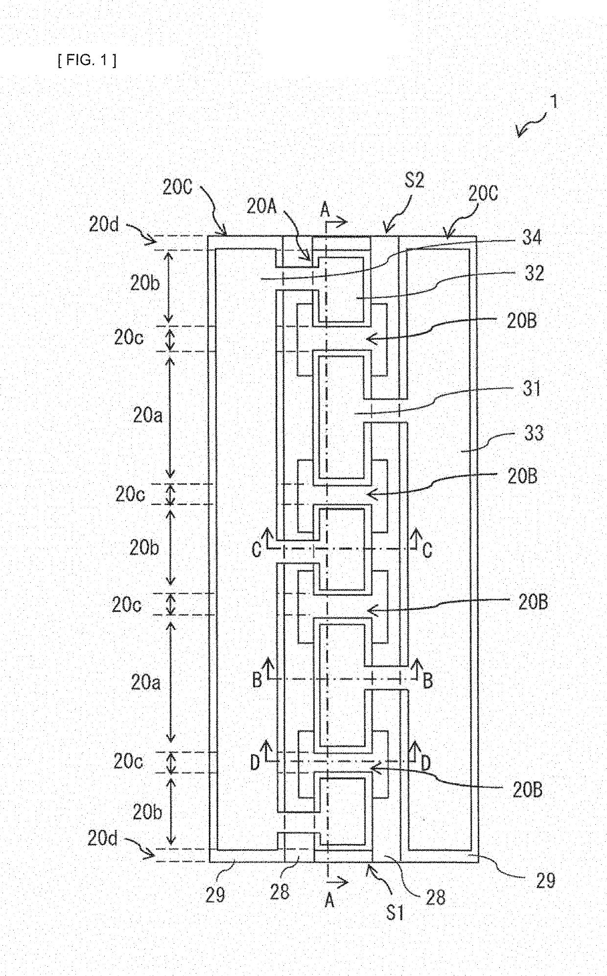
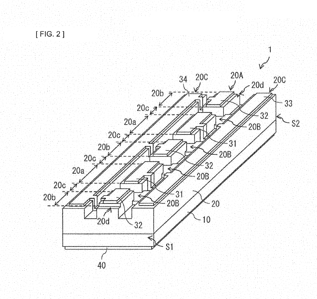
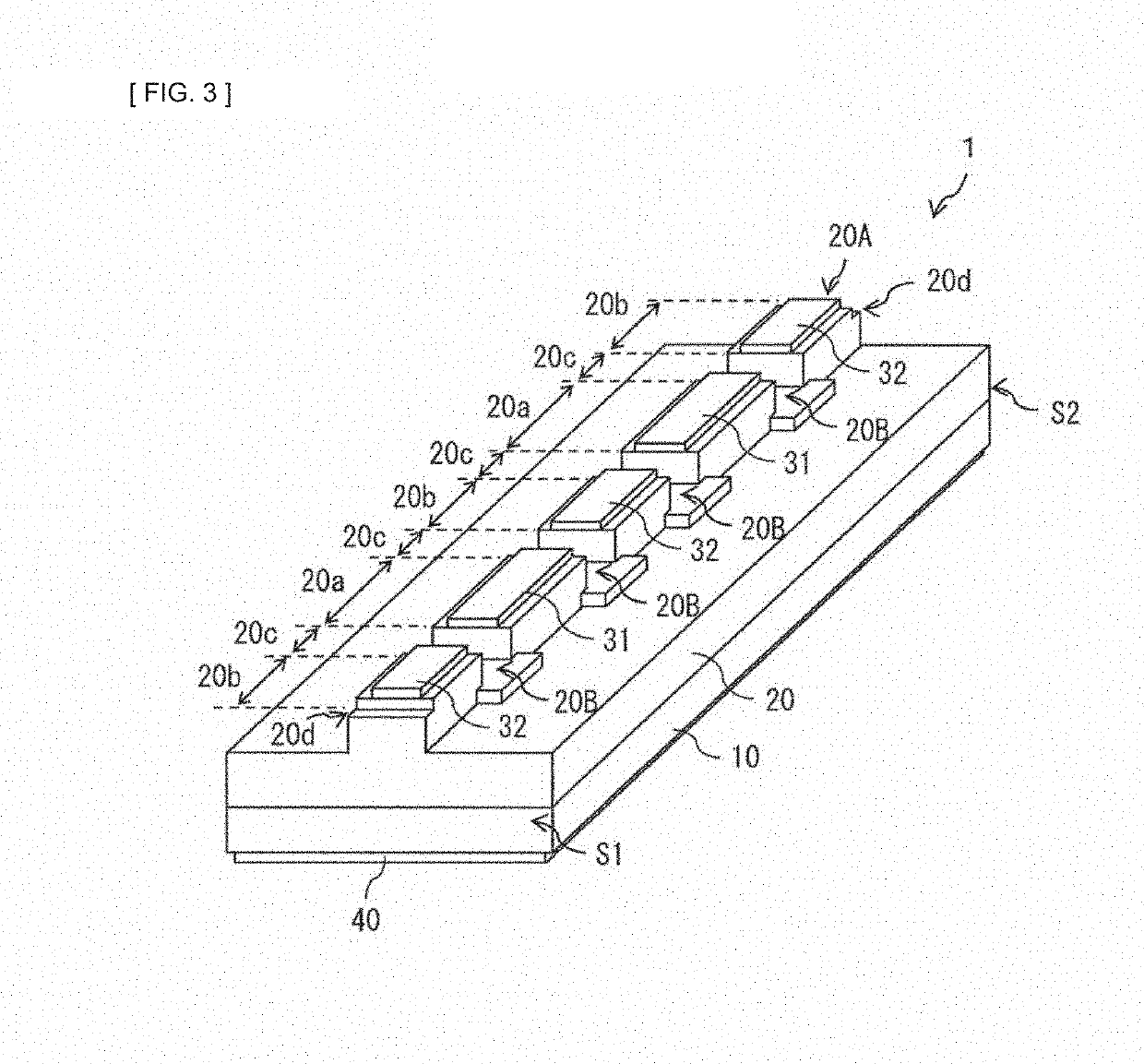
[0072]Description is given of a configuration of a semiconductor laser 1 according to a first embodiment of the present disclosure. FIG. 1 illustrates a configuration example of a top surface of the semiconductor laser 1 according to the present embodiment. FIG. 2 illustrates a perspective configuration example of the semiconductor laser 1 illustrated in FIG. 1. FIG. 3 illustrates a perspective configuration example of a portion of the semiconductor laser 1 illustrated in FIG. 1 excluding bank parts 20C (described later).

[0073]The semiconductor laser 1 is an element that generates an optical pulse, and is used suitably, for example, as a light source of a laser radar, a laser for processing, a medical laser scalpel, and the like. The semiconductor laser 1 is an edge-emitting laser. The semiconductor laser 1 includes a front end surface S1 and a rear end surface S2 that are opposed to each other in a resonator-direction, and a raised ridge part 20A int...


PUM


Abstract

In a semiconductor laser according to an embodiment of the present disclosure, a ridge part has a structure in which a plurality of gain regions and a plurality of Q-switch regions are each disposed alternately with each of separation regions being interposed therebetween in an extending direction of the ridge part. The separation regions each have a separation groove that separates from each other, by a space, the gain region and the Q-switch region adjacent to each other. The separation groove has a bottom surface at a position, in a second semiconductor layer, higher than a part corresponding to a foot of each of both sides of the ridge part.

Description

TECHNICAL FIELD[0001]The present disclosure relates to a semiconductor laser, an electronic apparatus, and a method of driving the semiconductor laser.BACKGROUND ART[0002]In a semiconductor laser, there is a Q-switch operation as a method of obtaining a high-power pulse by controlling oscillation. In the Q-switch operation, optical loss is initially increased to suppress oscillation, thereby facilitating optical pumping to cause the number of atoms in excited states to sufficiently increase; at that point in time, a Q-value is raised, thus allowing for oscillation. The semiconductor laser that allows for the Q-switch operation is described in the following PTLs 1 to 5, for example.CITATION LISTPatent Literature[0003]PTL 1: Japanese Unexamined Patent Application Publication No. H1-262683[0004]PTL 2: Japanese Unexamined Patent Application Publication No. H5-90700[0005]PTL 3: Japanese Unexamined Patent Application Publication No. H10-229252[0006]PTL 4: Japanese Unexamined Patent Applic...

Claims


Application Information

Patent Timeline
IPC IPC(8): H01S5/06H01S5/22H01S5/042H01S5/0625H01S5/323H01S5/30H01S5/02
CPCH01S5/0615H01S5/2202H01S5/0428H01S5/0625H01S5/32316H01S5/3086H01S5/0206H01S5/028H01S5/0425H01S5/02272H01S5/02469H01S2304/04H01S5/0287H01S5/0601H01S5/06253H01S5/0655H01S5/1003H01S5/1017H01S5/1039H01S5/2072H01S5/2086H01S5/209H01S5/22H01S5/3054H01S5/04256H01S5/0237
Inventor ONO, TOMOKIOOHATA, TOYOHARUKOYAMA, TAKAHIROTAKIGUCHI, MIKIOTANAKA, MASAYUKI
Owner SONY CORP
Why Eureka
Try Eureka