Insulating sheet, method of manufacturing the same, and method of manufacturing structure using the insulating sheet

Inactive Publication Date: 2013-06-13
KYOCERA CORP
View PDF82 Cites 18 Cited by
  • Summary
  • Abstract
  • Description
  • Claims
  • Application Information

AI Technical Summary

Benefits of technology

[0010]According to the configuration described above, it is possible to obtain an insulating sheet with

Problems solved by technology

Since the ceramic layer is formed by thermal spraying ceramics under high temperature conditions, ceramic particles grow under the high temperature conditions so that a particle size easily becomes large and a flatness of the ceramic layer is easily degraded.
In addi

Method used


Image

  • Insulating sheet, method of manufacturing the same, and method of manufacturing structure using the insulating sheet
  • Insulating sheet, method of manufacturing the same, and method of manufacturing structure using the insulating sheet
  • Insulating sheet, method of manufacturing the same, and method of manufacturing structure using the insulating sheet

Examples


first embodiment

[0025](Insulating Sheet)

[0026]Hereinafter, an insulating sheet according to a first embodiment of the invention will be described in detail with reference to the drawings.

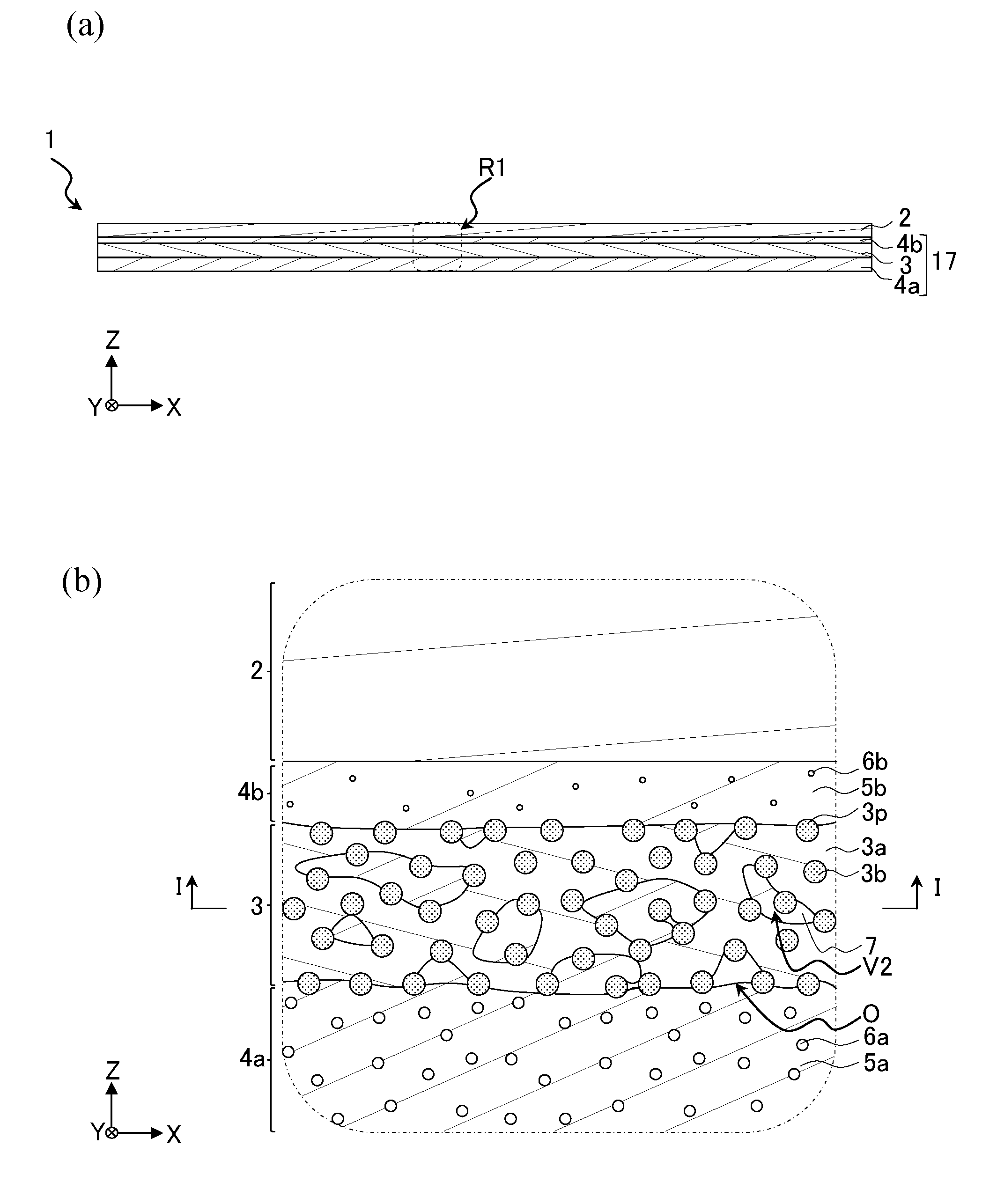
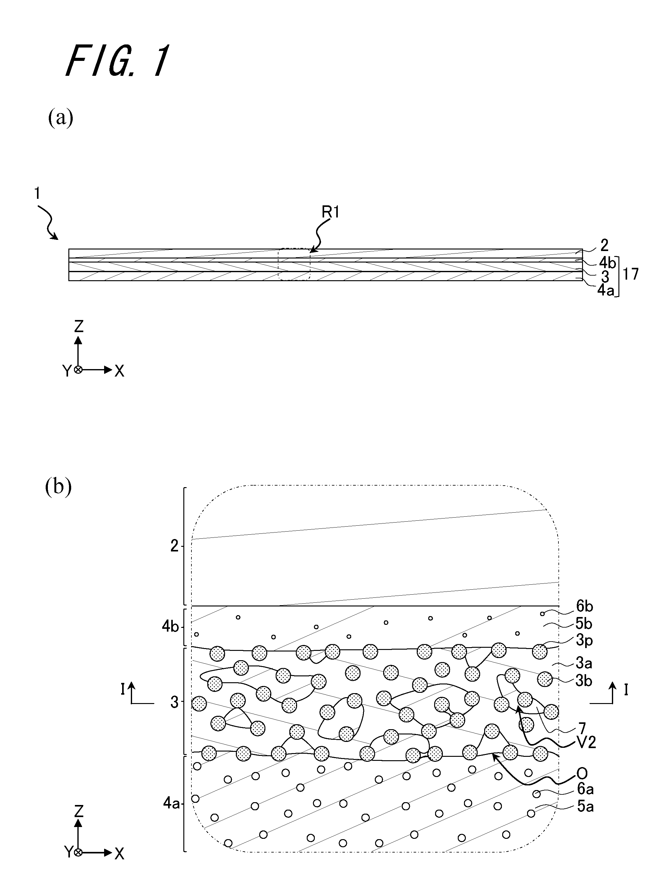
[0027]An insulating sheet 1 shown in FIG. 1(a) is used for manufacturing a wiring board 10 which will be described later, for example. The insulating sheet 1 includes a resin sheet 2, an inorganic insulating layer 3 disposed on the resin sheet 2, a first resin layer 4a disposed on the inorganic insulating layer 3, and a second resin layer 4b disposed between the resin sheet 2 and the inorganic insulating layer 3. The inorganic insulating layer 3, the first resin layer 4a and the second resin layer 4b in the insulating sheet 1 constitute an insulating layer 17 that remains in the wiring board 10 when manufacturing the wiring board 10 which will be described later.

[0028]The resin sheet 2 supports the inorganic insulating layer 3 when handling the insulating sheet 1, is removed from the inorganic insulating layer 3 wh...

second embodiment

[0160]Next, an insulating sheet according to a second embodiment of the invention will be described in detail with reference to FIG. 12. In addition, the same configuration as the first embodiment described above will be omitted.

[0161]In an insulating sheet 1A of the embodiment, the configuration thereof is different from the first embodiment, as shown in FIGS. 12(a) and 12(b), and voids and resin portions are not formed on an inorganic insulating layer 3A. In this case, it is possible that the inorganic insulating layer 3A have a low coefficient of thermal expansion, high rigidity, a high insulating property, and a low dielectric loss tangent.

[0162]The inorganic insulating layer 3A can be formed as follows, for example.

[0163]In the step (2), inorganic insulating sol is prepared so that a solid content of the inorganic insulating sol includes greater than 40% by volume and not greater than 80% by volume of first inorganic insulating particles 3aA and not less than 20% by volume and ...

third embodiment

[0164]Next, an insulating sheet according to a third embodiment of the invention will be described in detail with reference to FIG. 13. In addition, the same configuration as the first embodiment described above will be omitted.

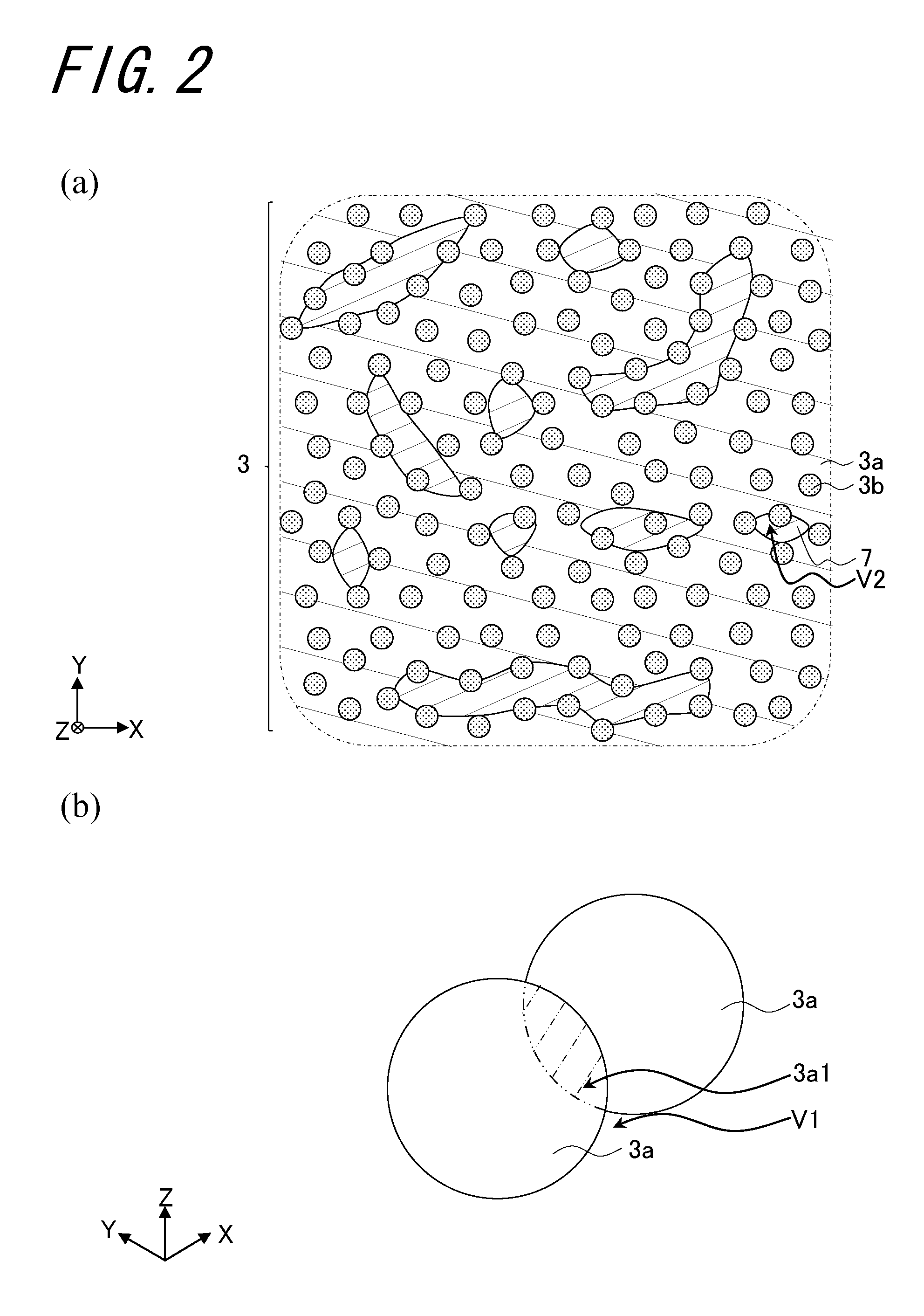
[0165]In an insulating sheet 1B of the embodiment, the configuration thereof is different from the first embodiment, as shown in FIGS. 13(a) and 13(b), and an inorganic insulating layer 3B does not include second inorganic insulating particles and is formed only of first inorganic insulating particles 3aB. As a result, it is possible to improve flatness of the inorganic insulating layer 3B.

[0166]In addition, in the insulating sheet 1B of the embodiment, the configuration there of is different from the first embodiment, and in the inorganic insulating layer 3B, third voids V3B which penetrate along the thickness direction are formed and resin portions 7B are arranged on the third voids V3B. As a result, when applying warping stress on the inorganic insulating ...


PUM

PropertyMeasurementUnit
Particle sizeaaaaaaaaaa

Abstract

An insulating sheet includes a resin sheet, and an insulating layer disposed on the resin sheet, wherein the insulating layer includes an inorganic insulating layer, and the inorganic insulating layer includes first inorganic insulating particles which have a particle size of not less than 3 nm and not greater than 110 nm and which are bonded to each other.

Description

TECHNICAL FIELD[0001]The present invention relates to an insulating sheet used for various things such as electronic devices (for example, various audio visual devices, household electrical appliances, communication devices, a computer and peripheral devices thereof), a transport aircraft, buildings and the like, a method of manufacturing the insulating sheet, and a method of manufacturing a structure using the insulating sheet.BACKGROUND ART[0002]In the related art, a structure in which electronic components are mounted on a wiring board is used as a mounting structure of an electronic device.[0003]Japanese Unexamined Patent Publication JP-A 2-253941 (1990) discloses a wiring board manufactured by using a ceramic layer formed by thermal spraying ceramics onto metal foil.[0004]Since the ceramic layer is formed by thermal spraying ceramics under high temperature conditions, ceramic particles grow under the high temperature conditions so that a particle size easily becomes large and a...

Claims


Application Information

Patent Timeline
IPC IPC(8): H01B3/02
CPCB32B27/14Y10T428/2495H01L23/145H01L23/49822H01L23/49827H05K3/4602H05K3/4673H05K2201/0175H05K2201/0195H05K2201/0209H01L2224/16227H01B3/02H05K2201/0129B32B2255/10B32B2255/26B32B2457/00H01L2224/16225Y10T428/25B32B2264/10H01L2924/00014H01L2224/0401B32B9/00H01B3/00H05K1/03H05K3/46
Inventor HAYASHI, KATSURA
Owner KYOCERA CORP
Why Eureka
Try Eureka