Wafer-level intrapixel getter reflector whole die encapsulation device and method

a reflector and reflector technology, applied in the field of high density focal plane arrays, can solve the problems of insufficient package vacuum over the required lifetime of the sensor, and the non-imaging area typically used for thin film getters, so as to reduce non-imaging areas and improve sensor performance. the effect of performan

Active Publication Date: 2013-06-20
BAE SYST INFORMATION & ELECTRONICS SYST INTERGRATION INC
View PDF3 Cites 8 Cited by
  • Summary
  • Abstract
  • Description
  • Claims
  • Application Information

AI Technical Summary

Benefits of technology

[0003]To solve this problem, the functions of the thin film getter and the quarter wave reflector already in the pixel structure are combined. The thin film getter comprises generally opaque, reflective metals that can be used as the “reflector” material in microbolometer pixel structures. This allows the thin film getter material to be placed within the imaging array without degrading sensor performance and still providing gettering function as FPAs are miniaturized by reducing non-imaging areas. Therefore, the thin film getter is placed under the sensor pixels, providing sufficient area for the thin film getter to maintain package vacuum life.

Problems solved by technology

As refinements and innovative improvements are used to reduce the size of the overall focal plane array, the non-imaging area typically used for thin film getters become inadequate to maintain the package vacuum over the required lifetime of the sensor.

Method used


Image

  • Wafer-level intrapixel getter reflector whole die encapsulation device and method
  • Wafer-level intrapixel getter reflector whole die encapsulation device and method
  • Wafer-level intrapixel getter reflector whole die encapsulation device and method

Examples


Embodiment Construction

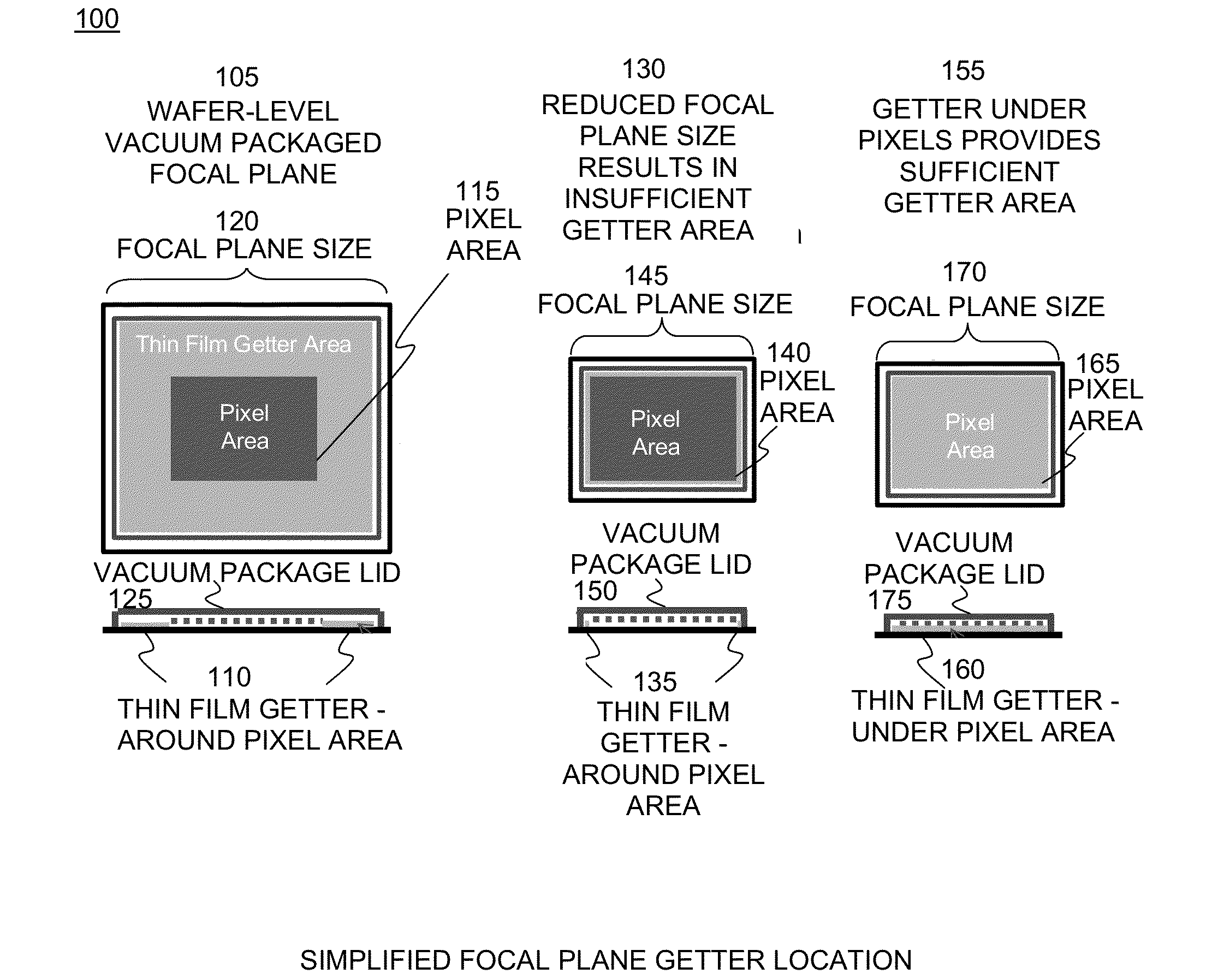
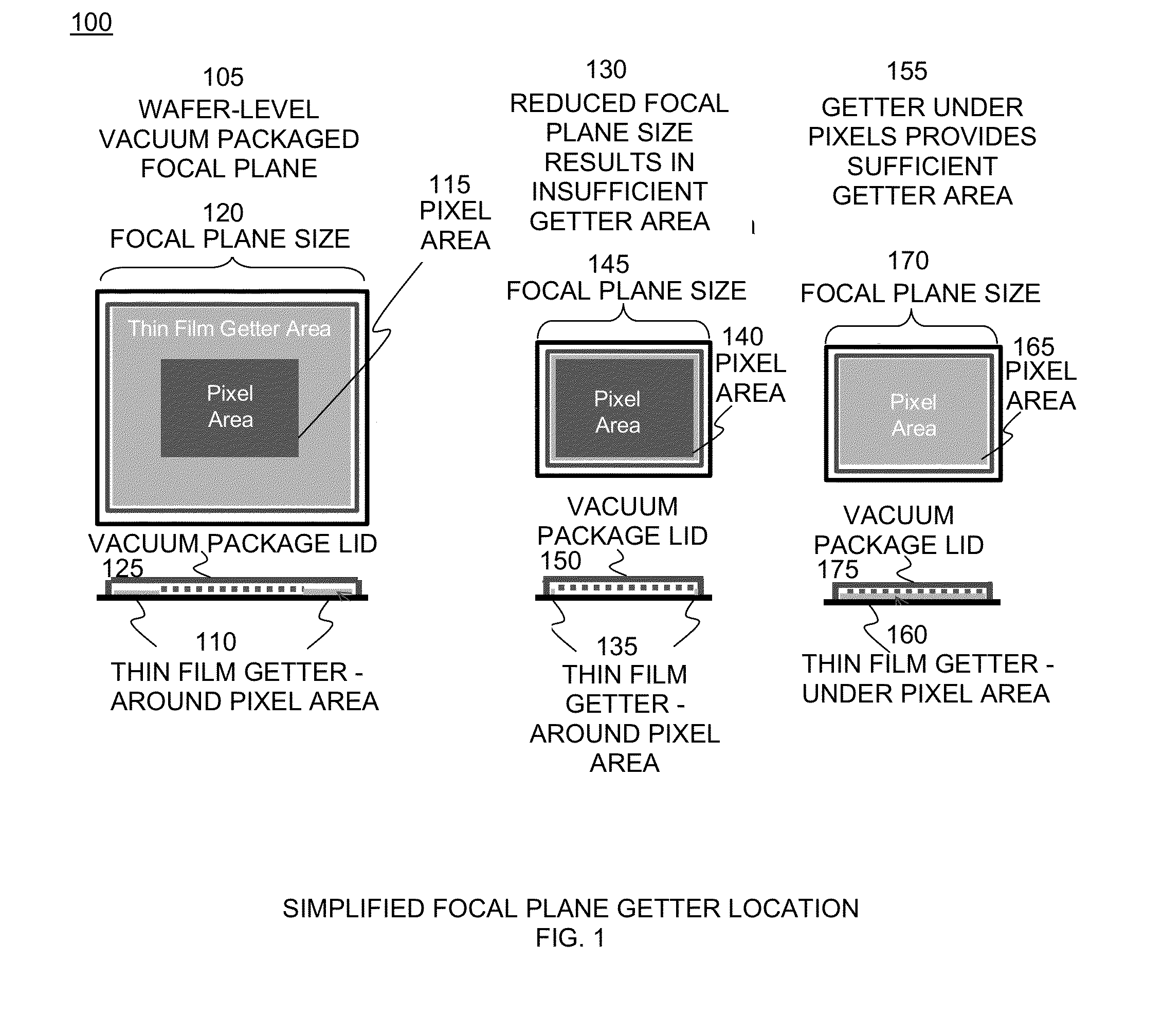
[0014]In wafer level vacuum packaging for microbolometers a thin film getter is used within the vacuum cavity to maintain low vacuum levels.

[0015]FIG. 1 depicts getter locations in wafer-level focal plane packages 100. A first wafer-level vacuum packaged focal plane 105 includes thin film getter 110 around pixel area 115. This results in a larger focal plane size 120. Capping the focal plane is vacuum package lid 125. Second wafer-level vacuum packaged focal plane 130 includes thin film getter 135 around pixel area 140. This results in a smaller focal plane size 145; however, this results in insufficient getter area to provide reliable sub-atmospheric pressure operation beneath focal plane vacuum package lid 150. Third wafer-level vacuum packaged focal plane 155 includes thin film getter 160 under pixel area 165. This results in a smaller focal plane size 170 while providing sufficient getter area for reliable sub-atmospheric pressure operation beneath focal plane vacuum package lid...


PUM


Abstract

An apparatus and method for a wafer level vacuum package uncooled microbolometer focal plane array (FPA) on a wafer level substrate with a thin film getter-reflector (G-R). The G-R removes gas from the vacuum package and is reflective in the frequency band of the FPA. Sensor pixels are supported about a quarter-wavelength above the G-R which is within the perimeter of the imaging array. The package is evacuated through a single aperture, and vacuum is maintained for the lifetime of the FPA. Imaging sensor size is reduced while maintaining resolution by reducing non-imaging area.

Description

FIELD OF THE INVENTION[0001]The present invention relates to high density focal plane arrays (FPAs), and more particularly, to microbolometer imaging arrays incorporating wafer-level multipurpose getter-reflectors (G-R).BACKGROUND OF THE INVENTION[0002]In wafer level vacuum packaging for microbolometers, a getter is used within the vacuum cavity to maintain low vacuum levels. The getter is currently placed in non-imaging areas of the focal plane so it does not interfere with the sensor operation. As refinements and innovative improvements are used to reduce the size of the overall focal plane array, the non-imaging area typically used for thin film getters become inadequate to maintain the package vacuum over the required lifetime of the sensor. A need exists for reduced thin film getter area in very small microbolometer arrays.BRIEF SUMMARY OF THE INVENTION[0003]To solve this problem, the functions of the thin film getter and the quarter wave reflector already in the pixel structur...

Claims


Application Information

Patent Timeline
Patent Type & Authority Applications(United States)
IPC IPC(8): H01L27/146H01L31/18
CPCH01L27/14634H01L27/14618H01L2924/0002G01J5/045G01J5/20H01L2924/00
Inventor BLACKWELL, JR., RICHARD J.
Owner BAE SYST INFORMATION & ELECTRONICS SYST INTERGRATION INC
Why Eureka
Try Eureka