Power semiconductor device

a technology of semiconductor devices and semiconductor chips, applied in semiconductor devices, solid-state devices, power conversion systems, etc., can solve the problems of difficult to reduce the chip size of the mosfet, and difficult to downsize the whole devi

Active Publication Date: 2013-06-20
MITSUBISHI ELECTRIC CORP
View PDF2 Cites 57 Cited by
  • Summary
  • Abstract
  • Description
  • Claims
  • Application Information

AI Technical Summary

Benefits of technology

[0014]In the above-described power semiconductor device, the first gate control signal is given, through the relay pattern, to the gate pad of the transistor arranged at the position farther from the first control circuit, and the second gate control signal is given, through the relay pattern, to the gate pad of the transistor arranged at the position farther from the second control circuit. Accordingly, an operation of wiring to the devices positioned farther from the first and second control circuits is easy.

Problems solved by technology

To deal with it, the current rating of the MOSFET has to be increased, which makes it difficult to reduce the chip size of the MOSFET.
Thus, there has been a problem that it is difficult to downsize the whole of a device.

Method used


Image

  • Power semiconductor device
  • Power semiconductor device
  • Power semiconductor device

Examples


embodiment

Preferred Embodiment

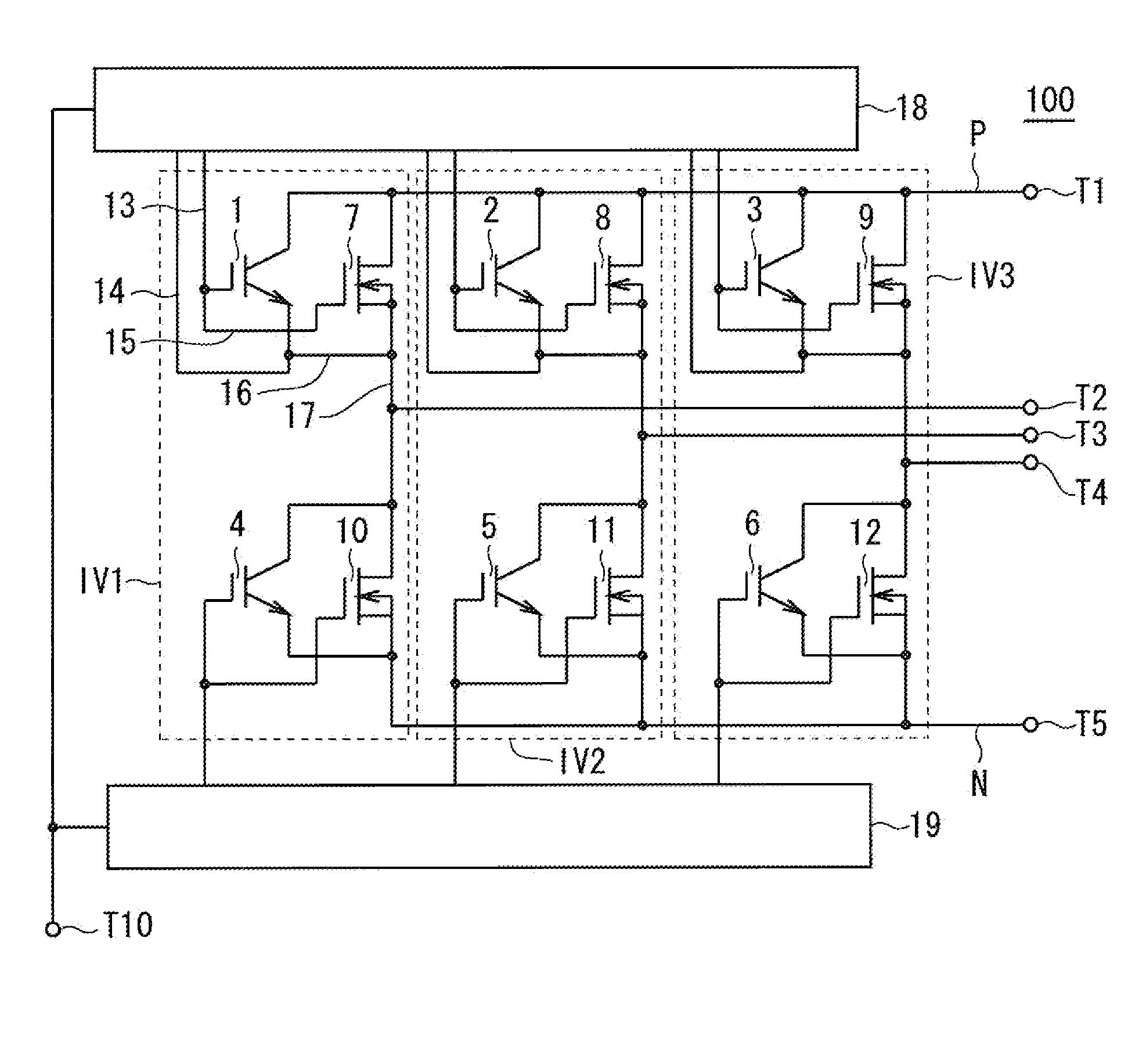
[0031]FIG. 1 shows a circuit configuration of a three-phase inverter module 100, as a preferred embodiment of a power semiconductor device according to the present invention.

[0032]The three-phase inverter module 100 shown in FIG. 1 includes three inverters IV1 to IV3.

[0033]The inverter IV1 includes MOSFETs (MOS field effect transistor) 7 and 10 and IGBTs (insulated gate bipolar transistor) 1 and 4, provided between a power supply line P and a power supply line N. The MOSFETs 7 and 10 are connected in series with each other. The IGBTs 1 and 4 are connected in parallel with the MOSFETs 7 and 10, respectively. The power supply line P is connected to a terminal T1 to which a power supply voltage is given. The power supply line N is connected to a terminal T5 to which a reference voltage is given. The source and drain of each of the MOSFETs 7 and 10 are commonly connected to a terminal T2. The IGBT 1 and the MOSFET 7 are switching devices at the high-potential side, a...


PUM


Abstract

Among first IGBTs and first MOSFETs, a transistor arranged near a first gate control circuit gives, through a gate thereof, a gate control signal supplied from the first gate control circuit to a gate of a transistor arranged at a position farther from the first gate control circuit. Among second IGBTs and second MOSFETs, a transistor arranged near a second gate control circuit gives, through a gate thereof, a gate control signal supplied from the second gate control circuit to a gate of a transistor arranged at a position farther from the second gate control circuit.

Description

BACKGROUND OF THE INVENTION[0001]1. Field of the Invention[0002]The present invention relates to a power semiconductor device, and particularly relates to a power semiconductor device in which an IGBT and a MOSFET operated in parallel are used as switching devices.[0003]2. Description of the Background Art[0004]In a switching device such as an IGBT (insulated gate bipolar transistor), a configuration in which a MOSFET (MOS field effect transistor) is connected in parallel with the IGBT for the purpose of reducing a switching loss has conventionally been studied.[0005]For example, Japanese Patent Application Laid-Open No. 4-354156 (1992) discloses, in FIG. 5, a configuration in which gates of an IGBT and a MOSFET connected in parallel with each other are commonly connected and they are driven by a common gate drive circuit.[0006]In a case where such a configuration is adopted, by making use of a difference between the threshold voltages of the IGBT and the MOSFET, turn-off characteri...

Claims


Application Information

Patent Timeline
Patent Type & Authority Applications(United States)
IPC IPC(8): H02M7/537
CPCH02M7/003H02M7/537H01L2924/1305H01L2924/13055H01L2924/13091H01L2924/30107H01L2224/49113H01L2224/48247H01L2224/48137H01L2924/00H01L2224/48139H02M1/088H02M1/0095H01L2224/48096H01L2224/49111H01L2924/00012H01L25/07H01L25/18H01L27/00H01L21/77
Inventor TANAKA, TOMOFUMIIWAGAMI, TORU
Owner MITSUBISHI ELECTRIC CORP
Why Eureka
Try Eureka