Textured surfaces and methods of making and using same
a technology of textured surfaces and textured surfaces, applied in the field of textured surfaces, can solve the problems of affecting the aesthetics or functional properties of the touch screen surface, affecting the user experience, and affecting the user's experience, etc., and achieve the effect of improving the fingerprint resistan
- Summary
- Abstract
- Description
- Claims
- Application Information
AI Technical Summary
Benefits of technology
Problems solved by technology
Method used
Image
Examples
example 1
Fabrication of Masks by Dewetting of Ni and Cu CUTMF Stacks
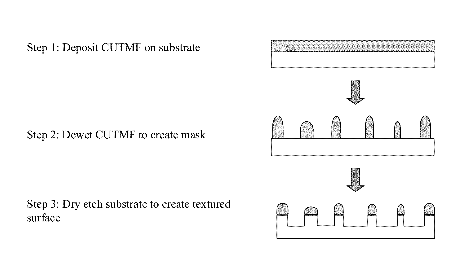
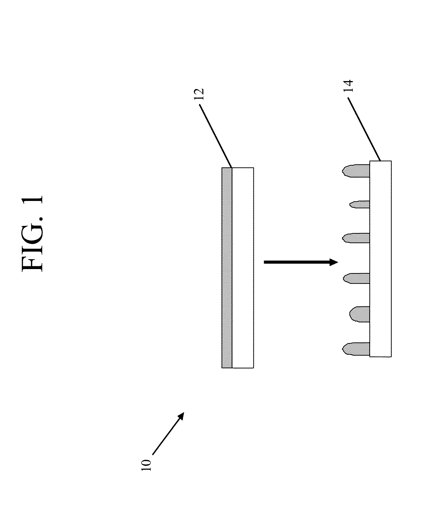
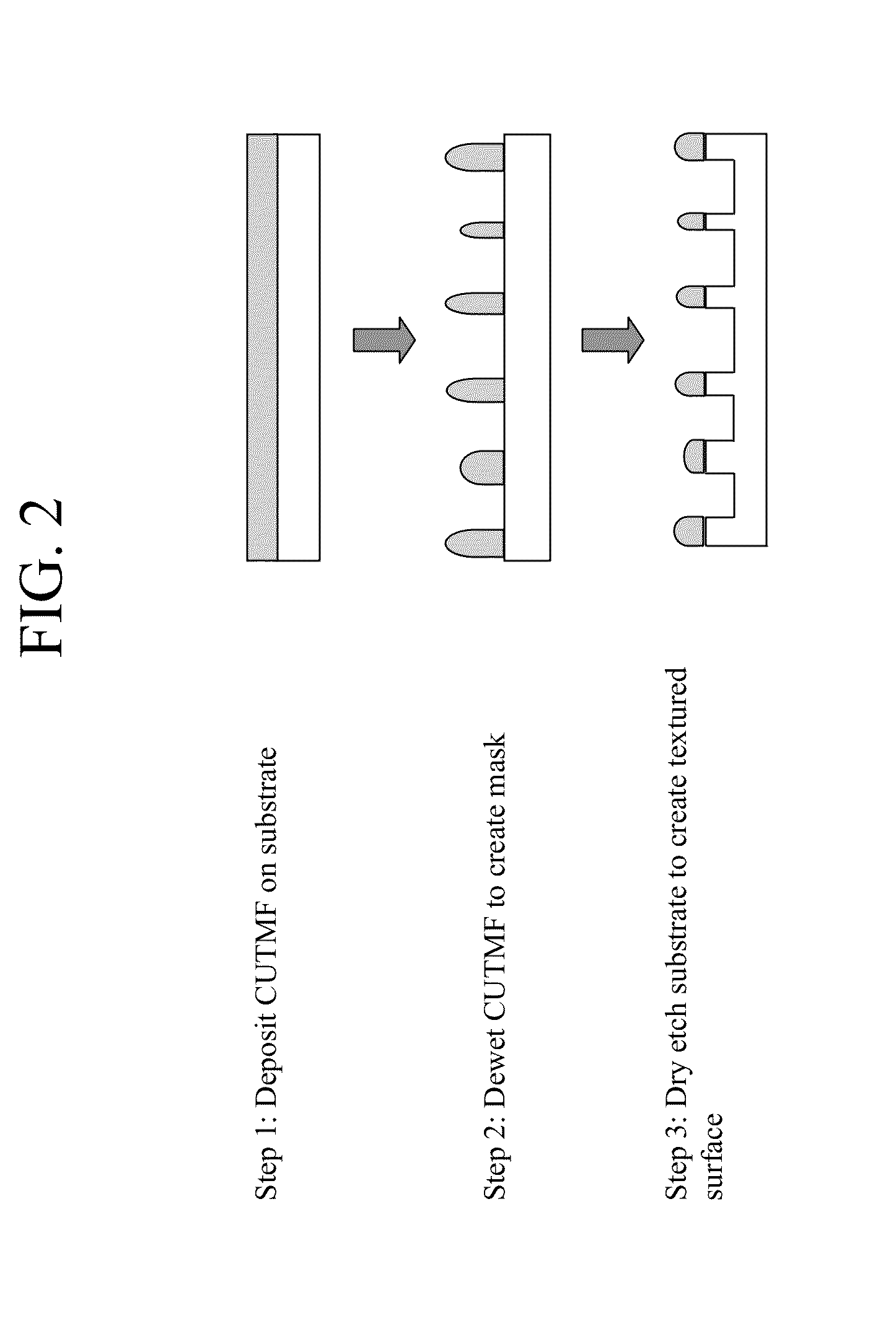
[0103]In this example, CUTMFs consisting of two layer stacks were prepared on flat glass substrates and dewetted under reduced pressure to produce masks for use in texturing the glass substrates.
[0104]The substrates chosen were non-strengthened flat glass sheets having a nominal composition of 69.2 mol % SiO2, 8.5 mol % Al2O3, 13.9 mol % Na2O, 1.2 mol % K2O, 6.5 mol % MgO, 0.5 mol % CaO, and 0.2 mol % SnO2.
[0105]The deposition of the CUTMFs was carried out using the sputtering system (ATC ORION-8-HV, AJA International) and procedures described in European Patent No. 2133921 Al and European Patent Application No. 09382238.5, which are incorporated herein by reference as if fully set forth below. The as-deposited CUTMFs comprised a layer of Ni, having an average thickness of about 1 nm, disposed on one surface of the glass samples, and a layer of Cu, having an average thickness of about 6 nm deposited thereon.
[0106]After the C...
example 2
Fabrication of Masks by Dewetting of Single Layer Cu CUTMFs
[0110]In this example, CUTMFs, which were single layers of Cu, were prepared on glass substrates and dewetted under reduced pressure conditions to produce masks for use in texturing the glass substrates.
[0111]The substrates chosen were about 1 inch by about 1 inch squares of fused silica glass.
[0112]The deposition of the CUTMFs was carried out using the sputtering system (ATC ORION-8-HV, AJA International) and procedures described in European Patent No. 2133921 Al and European Patent Application No. 09382238.5, which are incorporated herein by reference as if fully set forth below. The as-deposited Cu films had an average thickness of about 5 nm.
[0113]After the CUTMFs were formed, each sample was independently maintained in the sample holder of the sputtering system for the dewetting step. The samples were heated to about 450° C., at a rate of about 64° C. per minute. The samples were held at about 450° C. for about 20 minut...
example 3
Fabrication of Masks by Dewetting of Single Layer Cu CUTMFs
[0115]In this example, CUTMFs, which were single layers of Cu, were prepared on glass substrates and dewetted under ambient pressure conditions to produce masks for use in texturing the glass substrates.
[0116]The substrates chosen were about 2 inch by about 2 inch squares of non-strengthened flat glass sheets having a nominal composition of 69.2 mol % SiO2, 8.5 mol % Al2O3, 13.9 mol % Na2O, 1.2 mol % K2O, 6.5 mol % MgO, 0.5 mol % CaO, and 0.2 mol % SnO2.
[0117]The deposition of the CUTMFs was carried out using an in-line DC magnetron sputtering system (KDF903i, KDF Electronics) and using the procedures described in European Patent No. 2133921 A1 and European Patent Application No. 09382238.5, which are incorporated herein by reference as if fully set forth below. Each glass substrate was cleaned prior to film deposition. During each deposition step, 12 substrate pieces were placed on a 12 inch by 12 inch carrier pallet. The a...
PUM
| Property | Measurement | Unit |
|---|---|---|
| height | aaaaa | aaaaa |
| height | aaaaa | aaaaa |
| height | aaaaa | aaaaa |
Abstract
Description
Claims
Application Information
 - R&D
- Intellectual Property
- Life Sciences
- Materials
- Tech Scout
- Unparalleled Data Quality
- Higher Quality Content
- 60% Fewer Hallucinations
Browse by: Latest US Patents, China's latest patents, Technical Efficacy Thesaurus, Application Domain, Technology Topic, Popular Technical Reports.
© 2025 PatSnap. All rights reserved.Legal|Privacy policy|Modern Slavery Act Transparency Statement|Sitemap|About US| Contact US: help@patsnap.com


