Driving Circuit of a Liquid Crystal Panel and an LCD

Inactive Publication Date: 2013-06-27
TCL CHINA STAR OPTOELECTRONICS TECH CO LTD
View PDF6 Cites 13 Cited by
  • Summary
  • Abstract
  • Description
  • Claims
  • Application Information

AI Technical Summary

Benefits of technology

[0026]Contrast to the prior art, a suppression capacitor is placed between the second clock signal input and the controlling terminal. The suppression capacitor is used for lowering (or raising) the potential of the controlling terminal in response to a transition of the first clock signal from low potential to high potential and a transition of the second clock signal from high potentia

Problems solved by technology

The cost of the driving chip used in the conventional technology is high; in addition, it takes more time to attach the driving chip to the LCD panel during the p

Method used


Image

  • Driving Circuit of a Liquid Crystal Panel and an LCD
  • Driving Circuit of a Liquid Crystal Panel and an LCD
  • Driving Circuit of a Liquid Crystal Panel and an LCD

Examples


Example

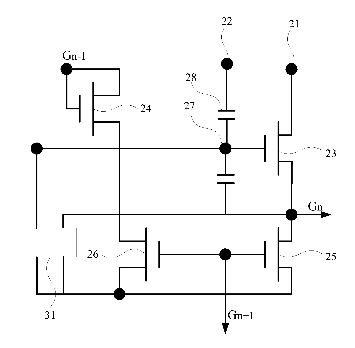
[0033]In all figures, units of similar structure are labeled with the same numbers.

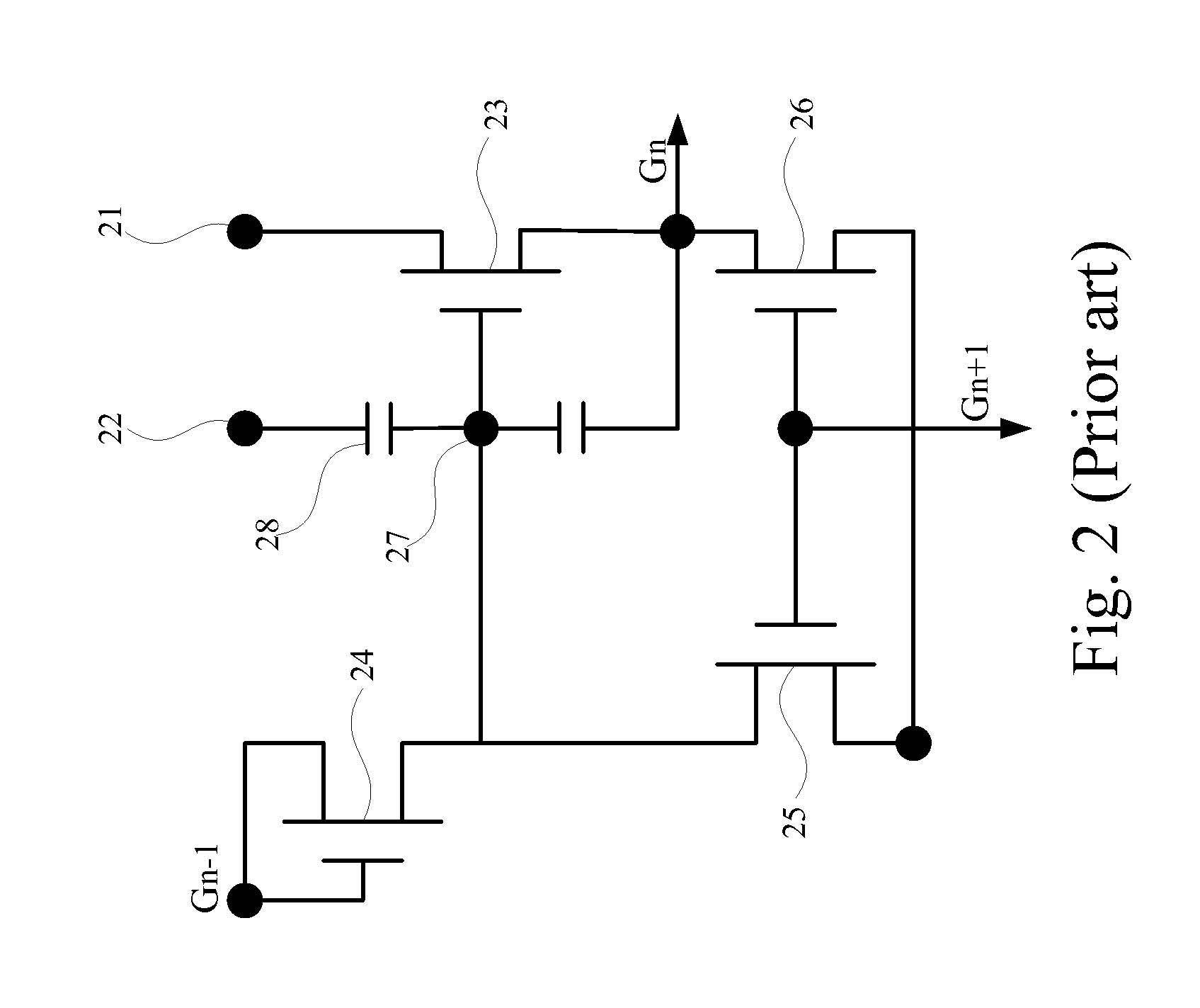
[0034]Referring to FIG. 2, FIG. 2 is a circuit diagram of a driving circuit of the LCD panel according to a preferred embodiment of the present invention.

[0035]The driving circuit of the LCD panel comprises a first clock signal input 21, a second clock signal input 22, a first TFT 23, a second TFT 24, a third TFT 25, a fourth TFT 26, a controlling terminal 27, and a suppression capacitor 28.

[0036]The first clock signal input 21 is connected to a source or drain (not shown) of the first TFT 23. The second clock signal input 22 is connected to the controlling terminal 27. The suppression capacitor 28 is placed between the second clock signal input 22 and the controlling terminal 27.

[0037]The controlling terminal 27 is connected to a gate (not shown) of the first TFT 23. The controlling terminal 27 is connected to the second TFT 24, the third TFT 25, and the fourth TFT 26.

[0038]Referring to FIG. 4, FIG. ...


PUM


Abstract

A driving circuit for use in an LCD is proposed. The driving circuit includes a first clock signal input, a second clock signal input, a first TFT, and a controlling terminal. The controlling terminal is connected to a gate of the first TFT. The first TFT is placed between the controlling terminal and the first clock signal input. The controlling terminal is placed between the first TFT and the second clock signal input. A parasite capacitor is formed in the first TFT. The driving circuit further includes a suppression capacitor placed between the second clock signal input and the controlling terminal. The suppression capacitor is used for adjusting a potential of the controlling terminal in response to transitions of the first clock signal and the second clock signal. The present invention provides a simplified layout, occupies less side area of the LCD, and upgrades image quality of the LCD.

Description

BACKGROUND OF THE INVENTION[0001]1. Field of the Invention[0002]The present invention relates to liquid crystal display (LCD) technology, and more particularly, to a driving circuit of a liquid crystal (LC) panel and an LCD.[0003]2. Description of the Prior Art[0004]With the development of LCD technology, a growing demand for high quality components inside the LCD panel is seen.[0005]Each pixel in an active-matrix liquid crystal display (AMLCD) comprises a thin-film transistor (TFT). A gate of the TFT is connected to a scan line, and a drain or source of the TFT is connected to a data line.[0006]High voltage is applied to the scan line (the gate), causing the TFT to be turned on. Grayscale voltage from the data line (source / drain) is applied to the LC layer through a transparent pixel electrode (drain / source). The grayscale voltage changes the alignment of the LCs in the LC layer, causing the predetermined grayscale to be shown.[0007]Enough positive voltage is applied to a scan line...

Claims


Application Information

Patent Timeline
IPC IPC(8): G09G3/36
CPCG09G2300/0408G09G3/3677
Inventor LI, SHIQILIN, SHIHCHYN
Owner TCL CHINA STAR OPTOELECTRONICS TECH CO LTD
Why Eureka
Try Eureka