Semiconductor-stacked substrate, semiconductor chip, and method for producing semiconductor-stacked substrate

a technology of semiconductor chips and substrates, applied in semiconductor devices, semiconductor devices, chemistry apparatus and processes, etc., can solve the problems of reducing the light-emitting efficiency of elements, and achieve the effect of reducing costs

Inactive Publication Date: 2013-07-04
PANASONIC INTELLECTUAL PROPERTY MANAGEMENT CO LTD
View PDF5 Cites 5 Cited by
  • Summary
  • Abstract
  • Description
  • Claims
  • Application Information

AI Technical Summary

Benefits of technology

[0019]According to the aspects disclosed in the specification, costs can be decreased.

Problems solved by technology

This effect decreases the probability of re-combination of the carriers in the light-emitting part so that this element is declined in light-emitting efficiency.

Method used


Image

  • Semiconductor-stacked substrate, semiconductor chip, and method for producing semiconductor-stacked substrate
  • Semiconductor-stacked substrate, semiconductor chip, and method for producing semiconductor-stacked substrate
  • Semiconductor-stacked substrate, semiconductor chip, and method for producing semiconductor-stacked substrate

Examples


exemplary embodiment 1

[0109]FIG. 10A is a view illustrating a principal surface of a semiconductor-stacked substrate of exemplary embodiment 1 according to the present invention. FIGS. 10B and 10C are cross-sectional views of the semiconductor-stacked substrate. In FIGS. 10A, 10B and 10C, the same reference numbers are attached, to the same constituents as in FIGS. 4A, 4B and 4C and FIGS. 6A, 6B and 6C.

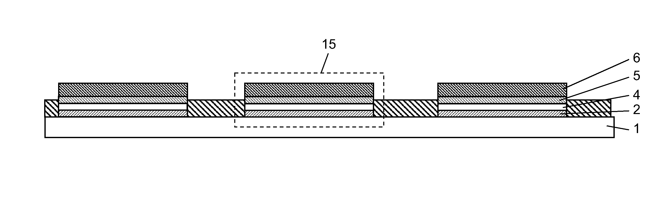
[0110]As illustrated in FIG. 10A, the semiconductor-stacked substrate of the present exemplary embodiment has a structure wherein a section or sections of semiconductor layer 15 made of an m-plane GaN, are formed on substrate 1 made of an m-plane sapphire substrate by crystal growth. When the section or each of the sections of semiconductor layer 15 is viewed from the principal surface side of substrate 1, the section of semiconductor layer 15 has a rectangular shape. One side thereof is parallel to a first axis, and a different side thereof is a second axis, which is orthogonal to the first axis. The firs...

exemplary embodiment 2

[0157]In the present exemplary embodiment, the sizes D1 and D2 in FIGS. 11A, 11B and 11C drawn for exemplary embodiment 1, i.e., the size D1 in the first axis direction of each of the sections of semiconductor layer 15 and the size D2 in the second axis direction thereof are defined as the following mathematical formulas 4 and 5 on the basis of the curvature radius ρ1 in the first axis direction, and that ρ2 in the second axis direction:

[Math. 4]

D1≅√{square root over (8Hmaxρ1)}  Mathematical formula 4

[Math. 5]

D2≅√{square root over (8Hmaxρ2)}  Mathematical formula 5

[0158]In the formulas, Hmax represents the maximum deformation amount of the semiconductor layer section, and the value thereof can be set to a desired deformation amount. When the value is set to, for example, the focal depth of the light-exposure device, the light exposure can be attained without receiving any restriction based on a deformation of the substrate.

[0159]For example, in the case of growing a GaN semiconducto...

exemplary embodiment 3

[0162]FIGS. 14A and 14B are views illustrating a semiconductor wafer of exemplary embodiment 3 according to the present invention; and FIGS. 15A and 15B are each a view illustrating semiconductor chips of exemplary embodiment 3, or one thereof. FIG. 14A is a view illustrating a principal surface of semiconductor wafer 10 when semiconductor regions 16 are formed on substrate 1. FIG. 14B is a view illustrating the principal surface of one out of semiconductor regions 16 that has a plurality of semiconductor elements 11. FIG. 15A is a cross-sectional view illustrating a portion of a cross section along line 15A-15A in FIG. 14B. FIG. 15B is a cross-sectional view of one of the semiconductor chips of exemplary embodiment 3 according to the present invention.

[0163]The semiconductor chips according to the present exemplary embodiment are each produced by use of any one of the semiconductor-stacked substrates produced in exemplary embodiments 1 and 2. As illustrated in FIG. 14A, a plurality...


PUM


Abstract

Disclosed is a semiconductor-stacked substrate having a substrate, and a plurality of semiconductor layers which are different in thermal expansion coefficient from the substrate, and are formed in a plurality of regions of a surface of the substrate, respectively. Each semiconductor layer has a growth plane that is a nonpolar plane or a semi-polar plane, and has different thermal expansion coefficients between along a first axis and a second axis orthogonal to each other and parallel to the surface of the substrate. The following mathematical formula 1 is satisfied. D1 and ρ1 represent, respectively, the length and the curvature radius of the semiconductor layer in a direction which passes through a point where the deformation amount of the semiconductor layer is largest and is parallel to the first axis direction. D2 and ρ2 represent those of the second axis direction.
Mathematicalformula10.8D1D2ρ1ρ21.2D1[Math.1]

Description

TECHNICAL FIELD[0001]The present invention relates to a semiconductor-stacked substrate and a semiconductor chip each having a plurality of semiconductor-stacked structures different in thermal expansion coefficient from a substrate thereof, and a method for producing the semiconductor-stacked substrate.BACKGROUND ART[0002]Nitride semiconductors having nitrogen (N) as a Group V element have been regarded as being promising materials of short-wavelength light-emitting elements because of the magnitude of the band gap thereof. Of these semiconductors, gallium nitride based compound semiconductors (GaN based semiconductors) have been actively researched. Blue light-emitting diodes (LEDs), green LEDs, and semiconductor lasers each made of a GaN based semiconductor have also been put into practical use (see, for example, PTLs 1 and 2 listed below).[0003]The GaN based semiconductors have a wurtzite type crystal structure. FIG. 1 illustrates unit lattices of GaN schematically. In a crystal...

Claims


Application Information

Patent Timeline
Patent Type & Authority Applications(United States)
IPC IPC(8): H01L29/205
CPCC30B29/406H01L33/007H01L21/02381H01L21/0242H01L21/02458H01L29/2003H01L21/0262H01L21/02639H01L29/205H01L29/868H01L21/0254
Inventor IWANAGA, JUNKOCHOE, SONGBAEKYOKOGAWA, TOSHIYA
Owner PANASONIC INTELLECTUAL PROPERTY MANAGEMENT CO LTD
Why Eureka
Try Eureka