Method for surface mounting electronic component, and substrate having electronic component mounted thereon

Inactive Publication Date: 2013-07-11
ORMON CORP
View PDF46 Cites 2 Cited by
  • Summary
  • Abstract
  • Description
  • Claims
  • Application Information

AI Technical Summary

Benefits of technology

The present invention provides a method for surface mounting electronic components on a substrate without using solder material. This method helps to prevent cracks from occurring in the joint interface. Overall, this helps to improve the reliability and efficiency of electronic components.

Problems solved by technology

As a result, an area of a conductive circuit is reduced, which increases a risk of troubles such as a bonding failure due to insufficient supply of a solder material, or a short circuit between adjacent circuits due to protrusion of the solder material.
However, the above-mentioned packaging method has a limitation in miniaturization.
However, such a method increases a material cost incurred by forming the solder material or the like into a film shape or by using anisotropically conductive material, and a heating process cannot be eliminated.
As a result, such a method cannot cope with a demand for decreasing cost.
However, according to the foregoing method for surface mounting, there is a high risk for causing cracks in the interfaces between the electrode 510 of the electronic component 500 and the protruding electrode 450, and between the protruding electrode 450 and the metal fused portion 460, during the process of applying the ultrasonic vibration.
However, the flow of these sequences does not take place in an entire joint interface simultaneously, but there is a case where even a portion in which bonding is completed is continuously subjected to a load generated by the ultrasonic vibration.
Accordingly, cracks tend to be caused near the bonded portion, because, generally, the welded portion has a large deformation strength.
Further, according to the foregoing method for mounting, the cost for forming the protruding electrode 450 having a protruding shape is high.

Method used


Image

  • Method for surface mounting electronic component, and substrate having electronic component mounted thereon
  • Method for surface mounting electronic component, and substrate having electronic component mounted thereon
  • Method for surface mounting electronic component, and substrate having electronic component mounted thereon

Examples


Embodiment Construction

[0039]Hereinafter, embodiments of the invention are described below with reference to the drawings. However, dimensions, materials, shapes, relative positions, and the like described in the embodiments are not purposed for limiting the scope of this invention thereto unless otherwise specifically described so. In embodiments of the invention, numerous specific details are set forth in order to provide a more thorough understanding of the invention. However, it will be apparent to one of ordinary skill in the art that the invention may be practiced without these specific details. In other instances, well-known features have not been described in detail to avoid obscuring the invention.

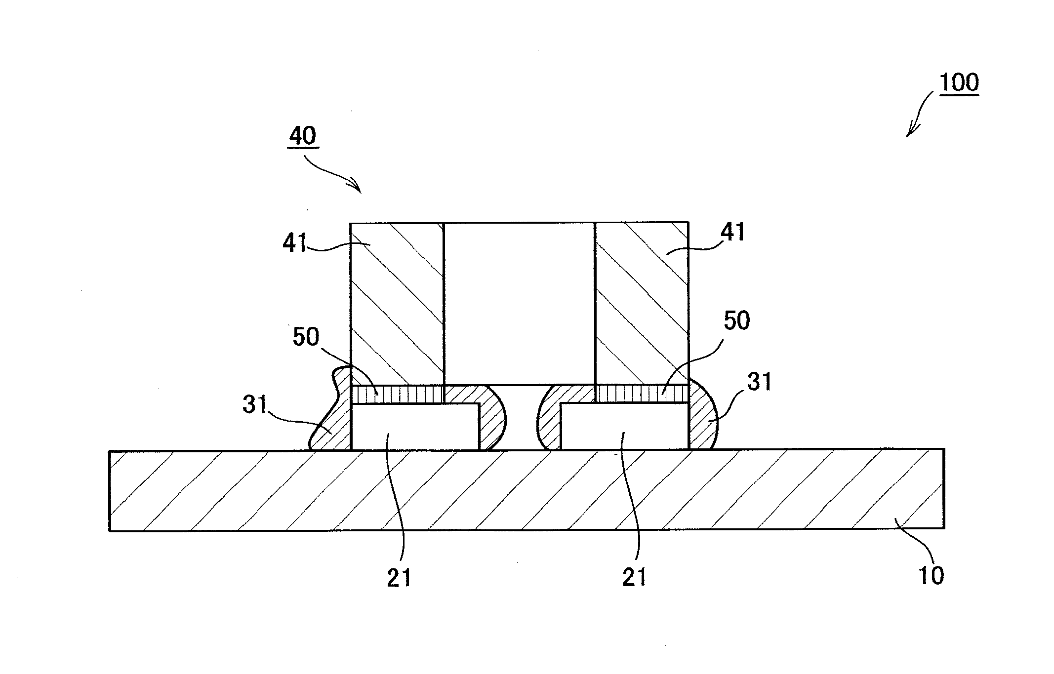
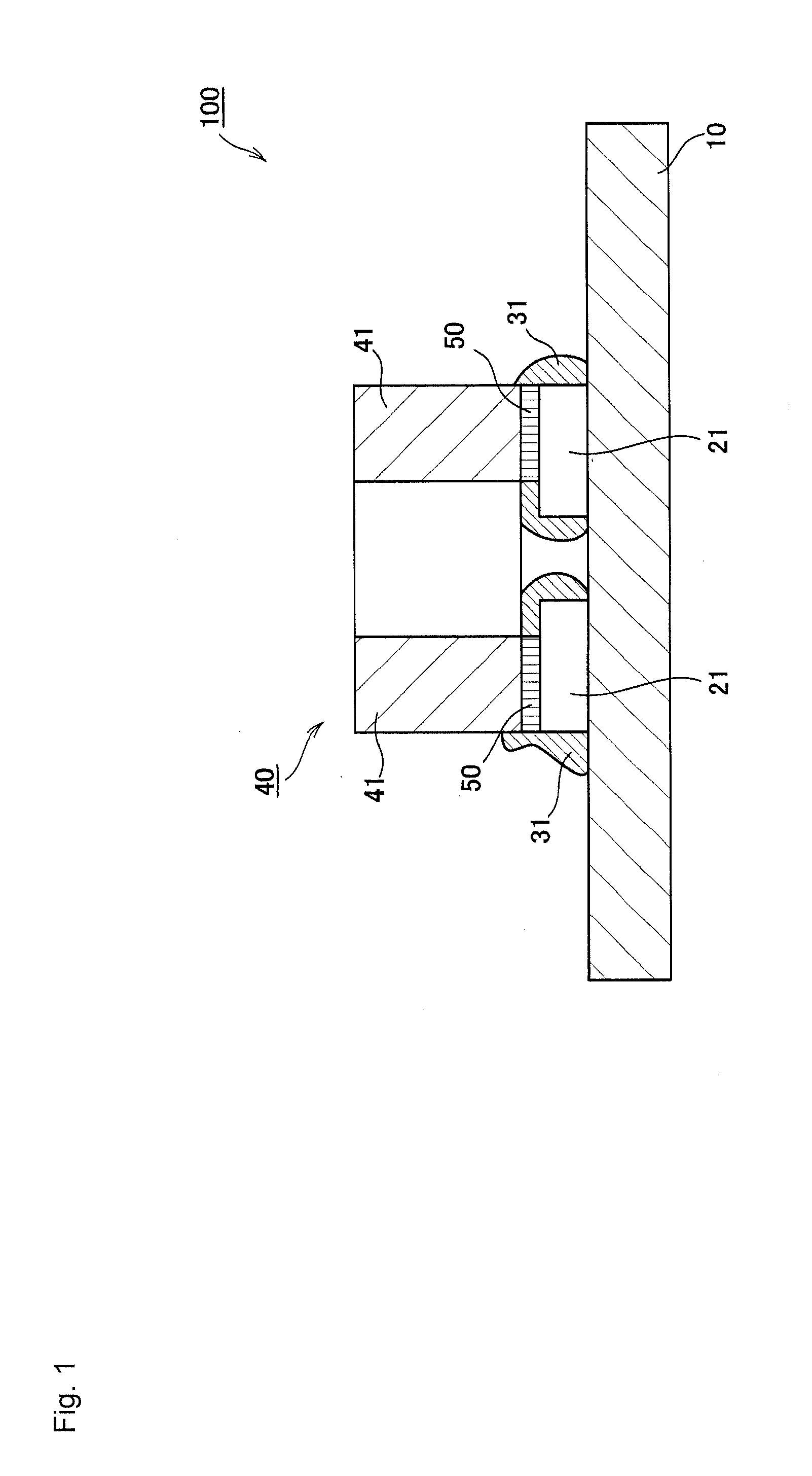
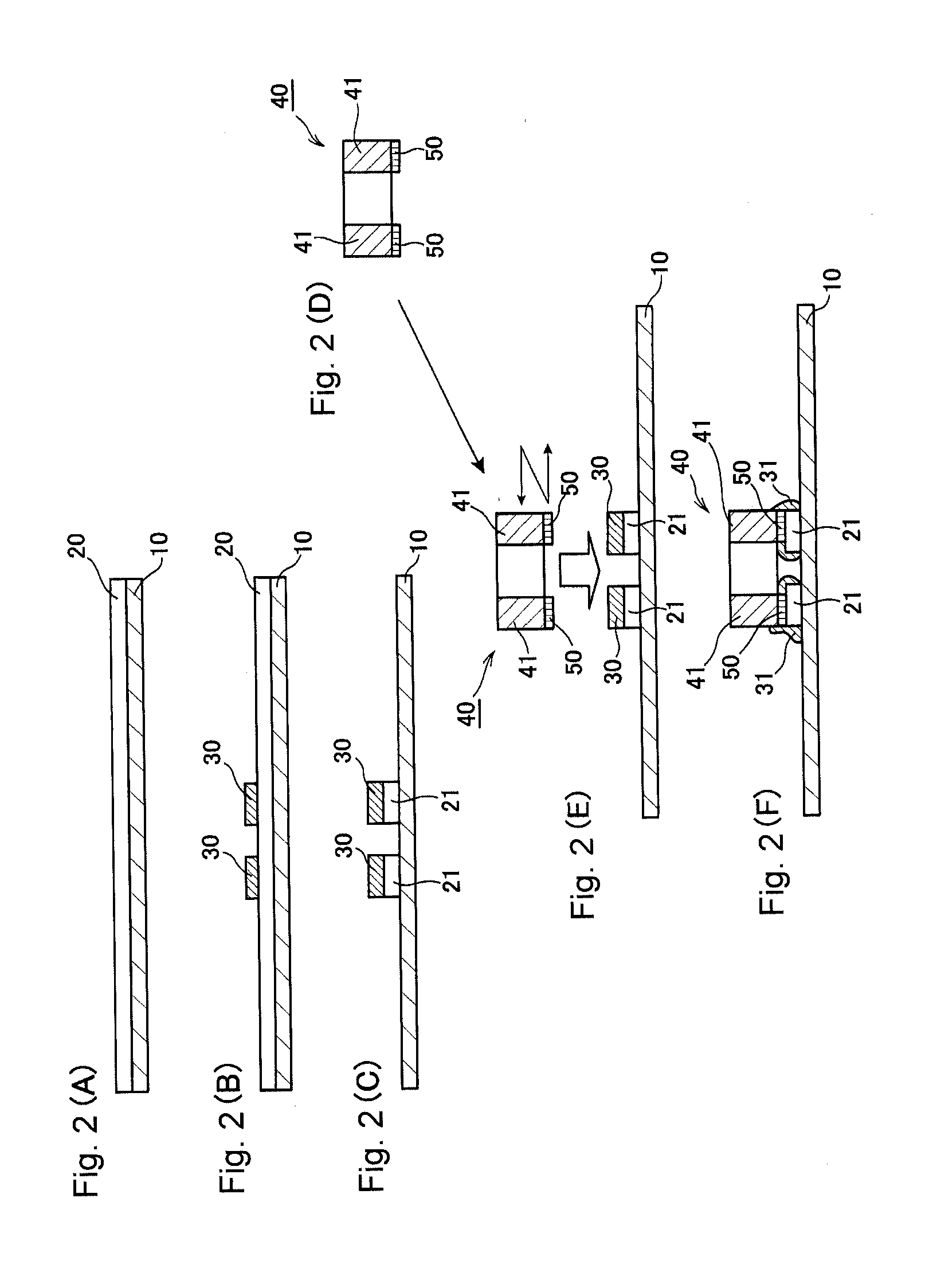
[0040]A description will be given of a method for surface mounting an electronic component, and a substrate having an electronic component mounted thereon according to one or more embodiments of the present invention, with reference to FIGS. 1 and 2.

[0041]Referring, in particular, to FIG. 1, a substrate...


PUM

PropertyMeasurementUnit
Hardnessaaaaaaaaaa
Shear strengthaaaaaaaaaa

Abstract

A method for surface mounting an electronic component includes providing a conductive circuit on a substrate member, forming a thermoplastic resin layer on a front surface of the conductive circuit, providing a surface of an electrode of an electronic component with a metal layer, and bonding the metal layer of the electronic component and the conductive circuit to each other by melting and partially removing a thermoplastic resin by applying a load generated by ultrasonic vibration that vibrates in a direction substantially parallel to a surface of the metal layer, while pressing the metal layer to the thermoplastic resin layer, and then stopping applying the load generated by the ultrasonic vibration, and hardening the thermoplastic resin thus melted by cooling. The metal layer is configured by a thin layer made of a material having a shear strength lower than that of a material constituting the conductive circuit.

Description

BACKGROUND[0001]1. Technical Field[0002]The present invention relates to a method for surface mounting an electronic component for surface mounting various types of electronic components such as a resistor or a capacitor on a printed wiring board on which a conductive circuit is formed, and a substrate having an electronic component mounted thereon.[0003]2. Background Art[0004]In general, a method using a solder material is used when various types of electronic components such as a resistor or a capacitor are surface mounted on a substrate.[0005]One conventional technique will be described with reference to FIG. 5. FIG. 5 is a process diagram illustrating surface mounting procedures according to Conventional Example 1. In this conventional example, a copper foil 220 having a thickness of about 12 μm to 35 μm is laminated on a surface of a base material 210 made of a heat-resistant glass epoxy resin or polyimide resin, and this is used as a substrate (see FIG. 5(A)). A conductive cir...

Claims


Application Information

Patent Timeline
IPC IPC(8): B32B37/04H05K1/11
CPCH01G2/06H01G4/228H05K3/06H05K3/244H05K3/305H05K2201/0129H05K2201/10636H05K2203/0571H05K2203/1189H05K2203/1461B32B37/04H05K1/11H05K3/32H05K2203/0285Y02P70/50
Inventor KAWAI, WAKAHIRO
Owner ORMON CORP
Why Eureka
Try Eureka