Method of manufacturing a display device

Active Publication Date: 2015-11-26
JAPAN DISPLAY INC
View PDF4 Cites 9 Cited by
  • Summary
  • Abstract
  • Description
  • Claims
  • Application Information

AI Technical Summary

Benefits of technology

The present invention provides a method for manufacturing a display device that prevents cracking in the horizontal direction. By etching the facing surfaces of adjacent portions of the first substrate during manufacturing, a gap between the surfaces can be created, which can prevent bending of the second substrate and reduce the risk of cracking. This method helps to create a safer and more reliable display device.

Problems solved by technology

However, when a subsequent breaking processing is performed, the one glass substrate has been already broken due to earlier breaking processing.
Accordingly, when the other glass substrate is bent in the subsequent breaking processing, if the one glass substrate which has been already broken is bent, there is a problem in that surfaces obtained by breaking may be brought into contact with each other and cracking may occur in a horizontal direction of a substrate surface.

Method used


Image

  • Method of manufacturing a display device
  • Method of manufacturing a display device
  • Method of manufacturing a display device

Examples


Embodiment Construction

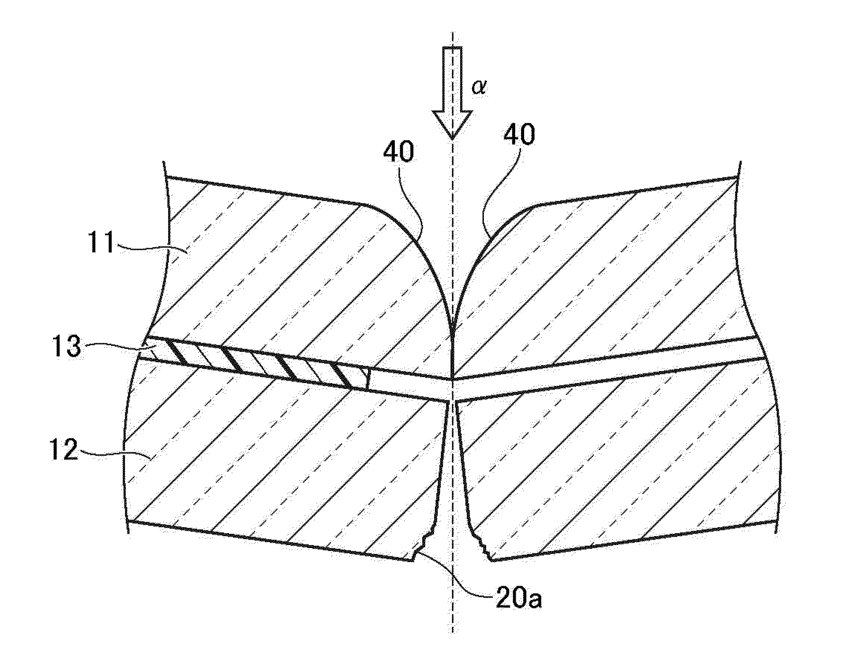
[0038]A method of manufacturing a display device according to an embodiment of the present invention may be applied to a method of manufacturing, for example, an organic light-emitting diode (OLED) display device, a liquid crystal display device, and the like. Hereinafter, descriptions will be made based on an example in which the method of manufacturing a display device according to the embodiment of the present invention is applied to a method of manufacturing an OLED display device.

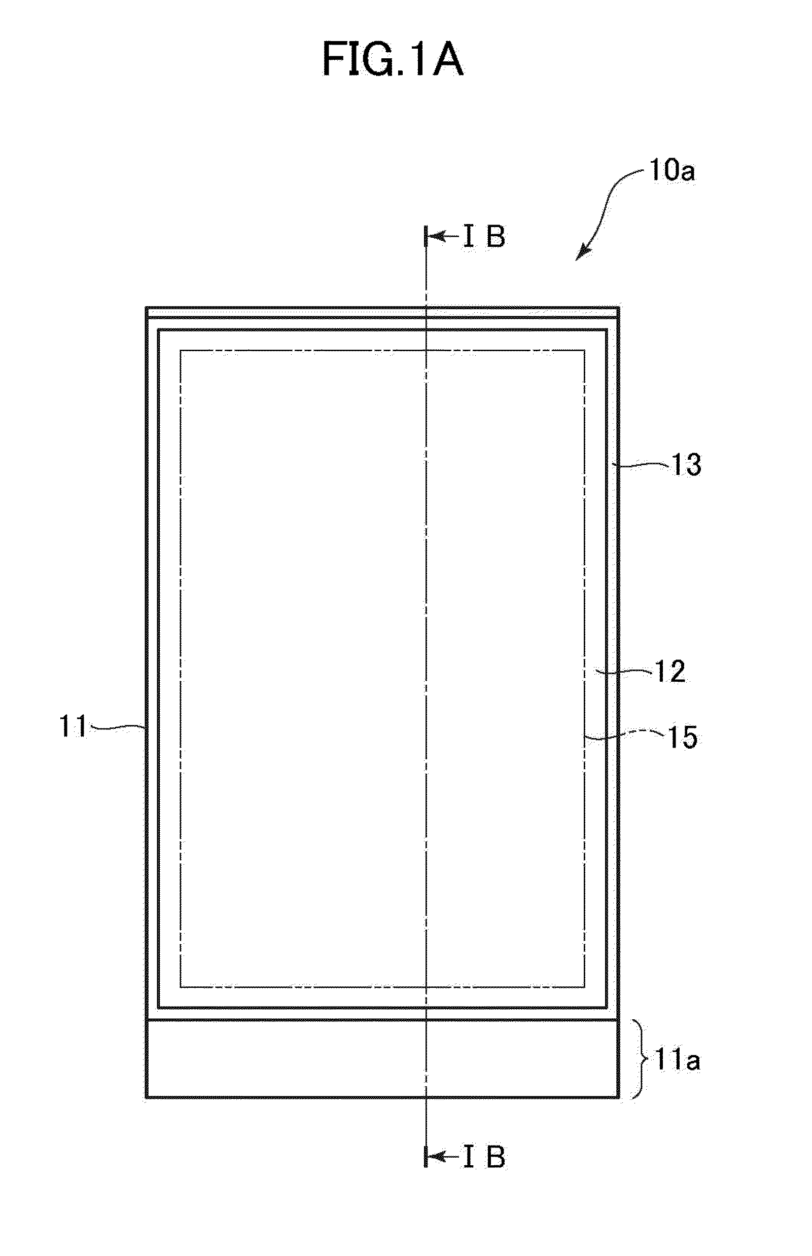
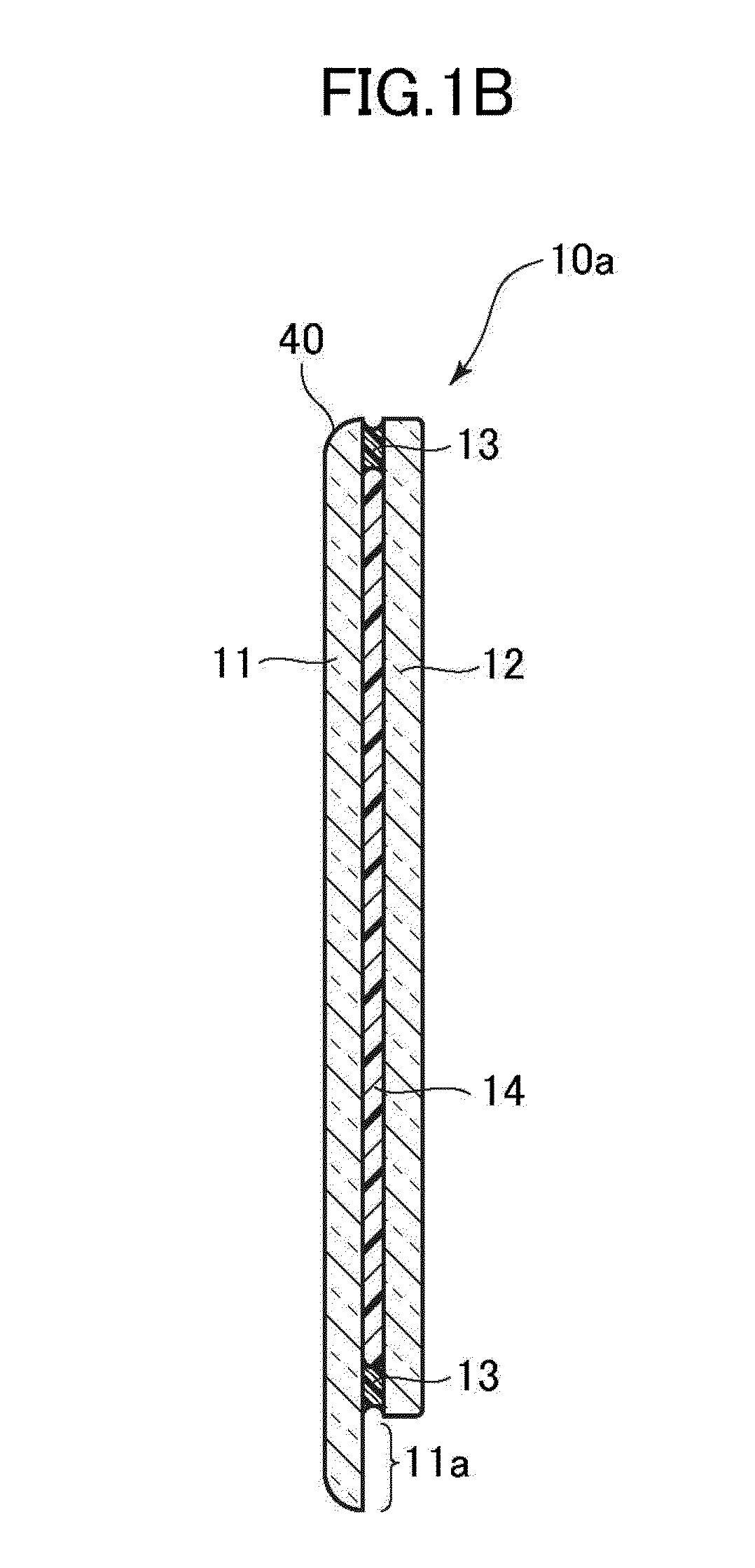
[0039]An OLED display device which is manufactured by the method of manufacturing a display device according to the embodiment of the present invention will be described with reference to FIGS. 1A and 1B. FIG. 1A is a plan view illustrating an example of the OLED display device which is manufactured by the embodiment of the present invention. FIG. 1B is a view illustrating a cross-section taken along a cutting plane line IB-IB in FIG. 1A.

[0040]The OLED display device 10a illustrated in FIGS. 1A and 1B ...


PUM

PropertyMeasurementUnit
Areaaaaaaaaaaa
Circumferenceaaaaaaaaaa

Abstract

A method of manufacturing a display device includes preparing a multilayout display panel which has a structure of a first substrate and a second substrate which are bonded to each other and is able to be cut into a plurality of products, scribing the first substrate, bending and breaking the scribed first substrate, performing thinning on the second substrate and the broken first substrate by chemical polishing, scribing the second substrate which is subjected to chemical polishing, and bending and breaking the scribed second substrate.

Description

CROSS-REFERENCE TO RELATED APPLICATION[0001]The present application claims priority from Japanese patent application JP2014-106973 filed on May 23, 2014, the content of which is hereby incorporated by reference into this application.BACKGROUND OF THE INVENTION[0002]1. Field of the Invention[0003]The present invention relates to a method of manufacturing a display device.[0004]2. Description of the Related Art[0005]Recently, in order to reduce the thickness and weight of a small or medium display, thinning of products is progressing. However, multiple production processing has been employed in order to improve productivity, and thus a thin film transistor substrate or a color filter substrate for manufacturing a multilayout panel has become larger. For this reason, it is difficult to reduce the thickness of the panel because the strength of a multilayout panel has to be maintained. Thus, in order to handle reduction in the thickness, the panel thickness of a multilayout panel is decr...

Claims


Application Information

Patent Timeline
IPC IPC(8): H01L51/56C03B33/02H01L51/52C03C15/02
CPCH01L51/56C03C15/02H01L2251/566H01L51/5246C03B33/02G02F1/1333G02F1/133351H10K59/8722H10K71/00B28D5/0011C03B33/033C03B33/076Y02P40/57H10K50/8426H10K71/851
Inventor SAKAMOTO, HIROTSUGUGUNJI, MASAKAZU
Owner JAPAN DISPLAY INC
Why Eureka
Try Eureka