Logic Elements Comprising Carbon Nanotube Field Effect Transistor (CNTFET) Devices and Methods of Making Same

a technology of field effect transistor and logic elements, which is applied in the direction of logic circuits characterised by logic functions, cad circuit design, and nano-informatics, etc., can solve the problems of high standby power dissipation at short channel lengths, and body effect can negatively impact the performance of cmos inverters

Active Publication Date: 2013-07-18
NANTERO
View PDF3 Cites 17 Cited by
  • Summary
  • Abstract
  • Description
  • Claims
  • Application Information

AI Technical Summary

Benefits of technology

[0013]The present disclosure relates to semiconductor logic elements, and more particularly to semiconductor logic elements comprising carbon nanotube field effect transistor devices (CNTFETs) and methods of making such elements. Such elements...

Problems solved by technology

The body effect can negatively impact the performance of the CMOS inverter by changing the threshold voltages of the n-channel MOSFET and the p-channel MOSFET.
The coplanar layout of the complementary MOSFETs coupled with the increasingly difficult scaling of MOSFETs to smaller sizes creates a barrier to reducing the amount of chip area consumed by the inverter circuits or NOT gates.
MOSFETs at the 90 nm technology node have high leakage currents resulting in high standby power dissipation at short channel lengths due to well-known problems associated with scaling FET devices threshold voltages.
In large ...

Method used


Image

  • Logic Elements Comprising Carbon Nanotube Field Effect Transistor (CNTFET) Devices and Methods of Making Same
  • Logic Elements Comprising Carbon Nanotube Field Effect Transistor (CNTFET) Devices and Methods of Making Same
  • Logic Elements Comprising Carbon Nanotube Field Effect Transistor (CNTFET) Devices and Methods of Making Same

Examples


Embodiment Construction

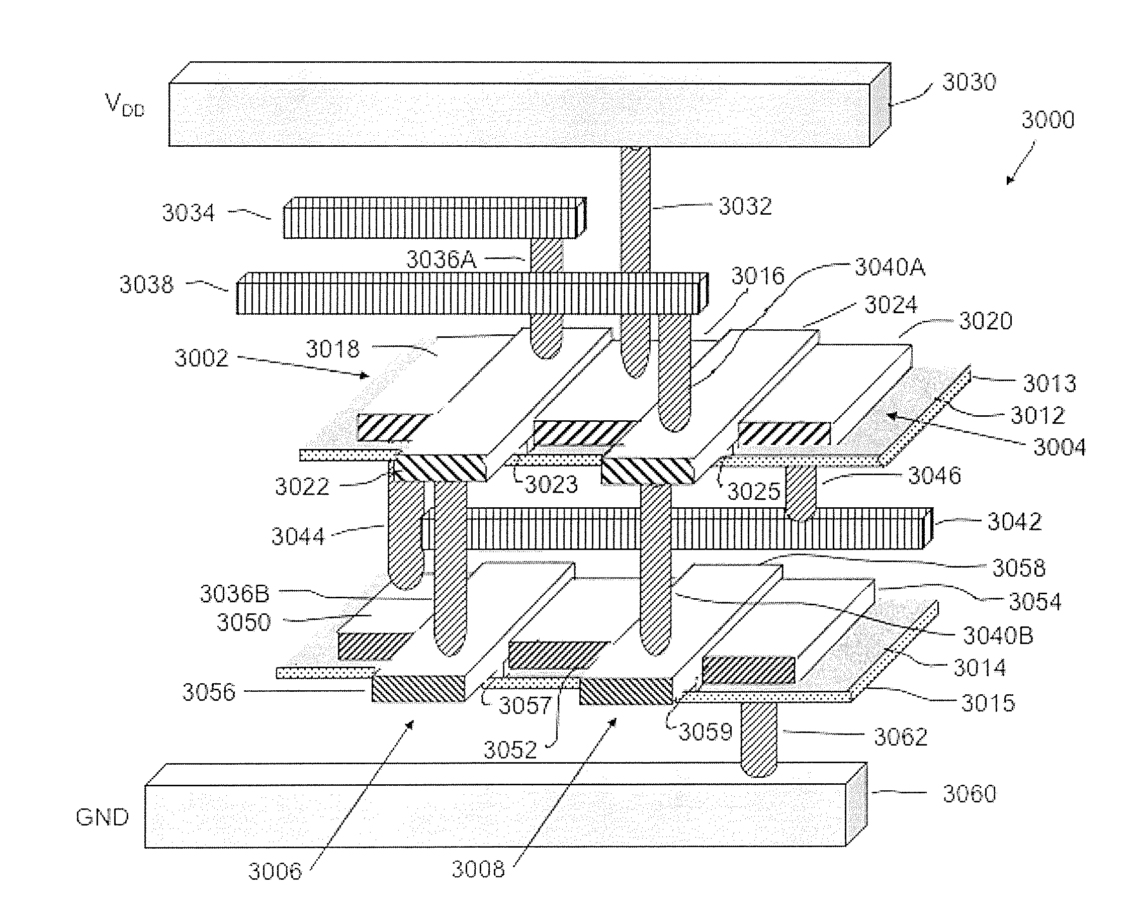
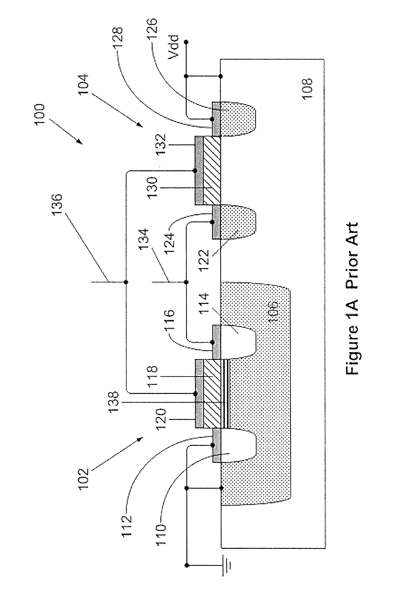
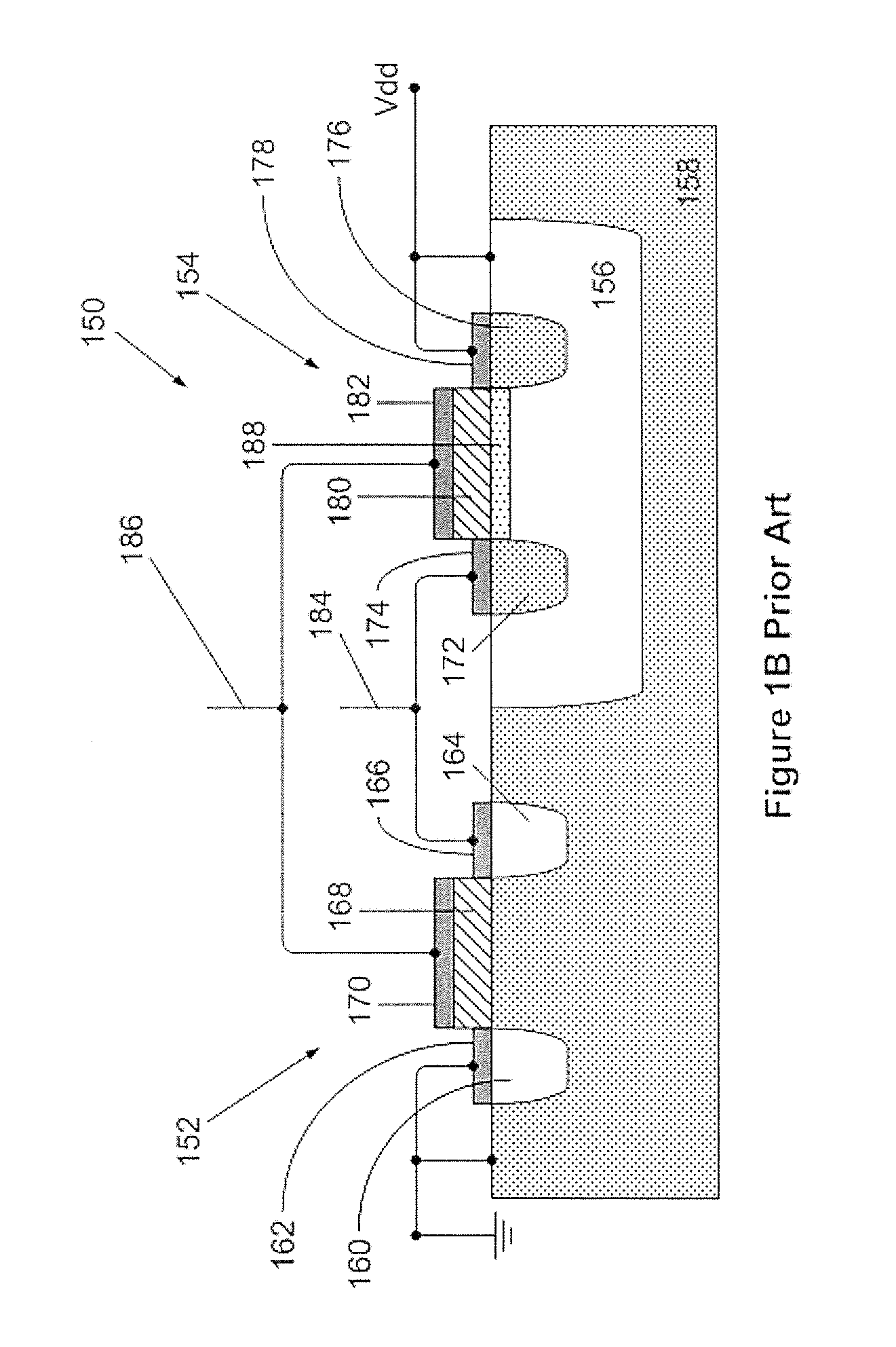
[0096]The present disclosure is directed toward NOT gates (or inverter circuits) and NAND circuits (or gates) fabricated using nanotube fabrics to replace semiconductor substrates. The NOT gates and NAND circuits can be constructed using carbon nanotube field-effect transistors (CNTFET) having nanotube fabrics as sources, drains, and channel regions. The nanotube fabric in each CNTFET is made of semiconducting carbon nanotubes to form either p-type, n-type, or ambipolar-type CNTFET devices. Therefore, parasitic components present in a MOSFET between p-type regions and n-type regions and the underlying semiconductor substrates are not present in CNTFETs. This is because the source, drain, and channel regions are formed in nanotube fabrics on insulating substrates, which replace semiconductor substrates and eliminates depletion region capacitances. Also, threshold modulation effects (body effects) of devices in series associated with semiconductor substrates, such as in NAND circuits ...


PUM


Abstract

Inverter circuits and NAND circuits comprising nanotube based FETs and methods of making the same are described. Such circuits can be fabricating using field effect transistors comprising a source, a drain, a channel region, and a gate, wherein the first channel region includes a fabric of semiconducting nanotubes of a given conductivity type. Such FETs can be arranged to provide inverter circuits in either two-dimension or three-dimensional (stacked) layouts. Design equations based upon consideration of the electrical characteristics of the nanotubes are described which permit optimization of circuit design layout based upon constants that are indicative of the current carrying capacity of the nanotube fabrics of different FETs.

Description

[0001]The present application claims the benefit of U.S. Provisional Patent Application No. 61 / 306,735, filed Feb. 22, 2010, the entire contents of which are incorporated herein by reference.TECHNICAL FIELD[0002]The present disclosure relates to semiconductor logic elements, and more particularly to semiconductor logic elements comprising carbon nanotube field effect transistor devices (CNTFETs) and methods of making such elements.BACKGROUND[0003]A traditional inverter circuit or NOT gate is constructed from two complementary switches connected in series and configured such that the switches are alternatively enabled. Metal-oxide-semiconductor field-effect transistors (MOSFET) are currently widely used in the fabrication of inverter circuits or NOT gates because their high input impedance results in low power dissipation after the MOSFETs are driven to enabled and disabled states, their low output impedance results in fast switching speeds for sharp edges, and their small size relat...

Claims


Application Information

Patent Timeline
IPC IPC(8): H01L29/78H01L29/16H01L21/02
CPCB82Y10/00H01L27/283H01L51/0048H01L51/0558Y10S977/742B82Y40/00H01L21/02376H01L29/16H01L29/78H03K19/20H10K19/10H10K85/221H10K10/484G06F30/30H10K10/84H10K10/488
Inventor BERTIN, CLAUDE L.
Owner NANTERO
Why Eureka
Try Eureka