Display device
a display device and active matrix technology, applied in non-linear optics, instruments, optics, etc., can solve the problems of increasing the area of the frame portion (a peripheral region over the substrate other than the pixel portion) and the small size of the active matrix display device. to achieve the effect of reducing the wiring resistance of the display devi
- Summary
- Abstract
- Description
- Claims
- Application Information
AI Technical Summary
Benefits of technology
Problems solved by technology
Method used
Image
Examples
embodiment mode 1
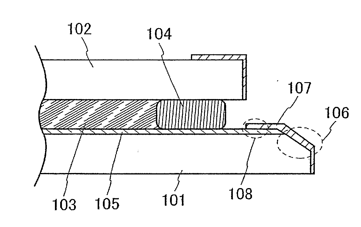
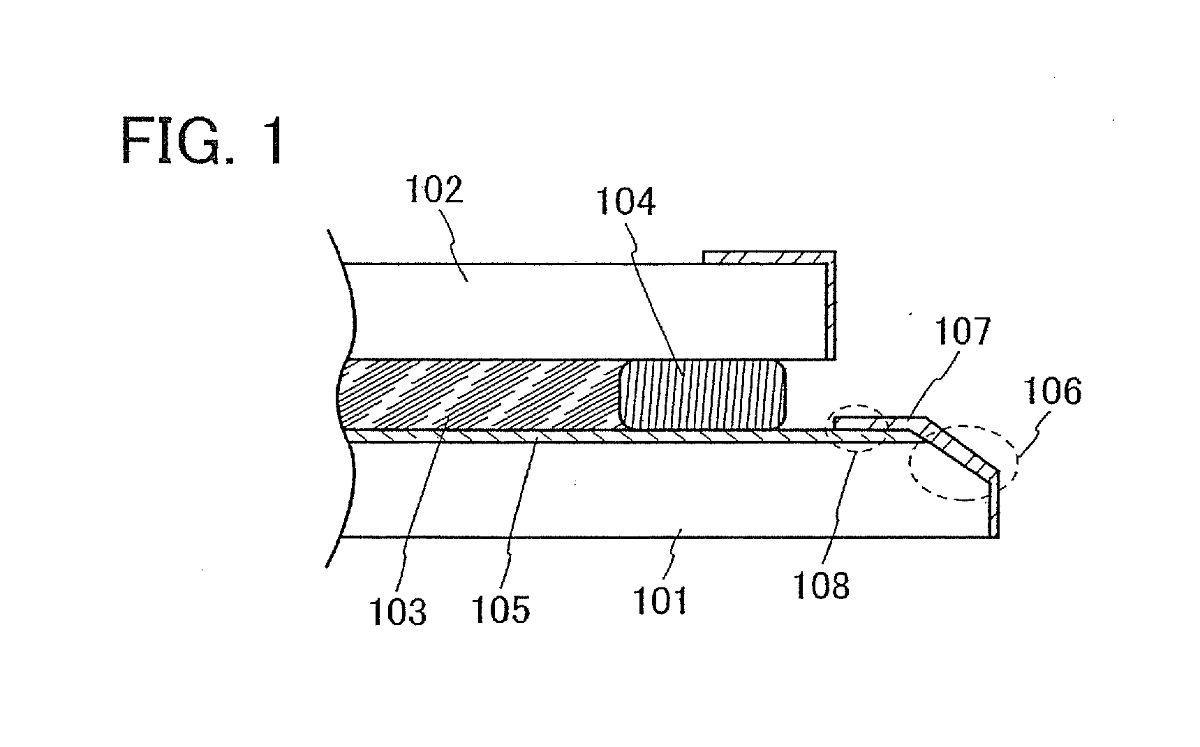
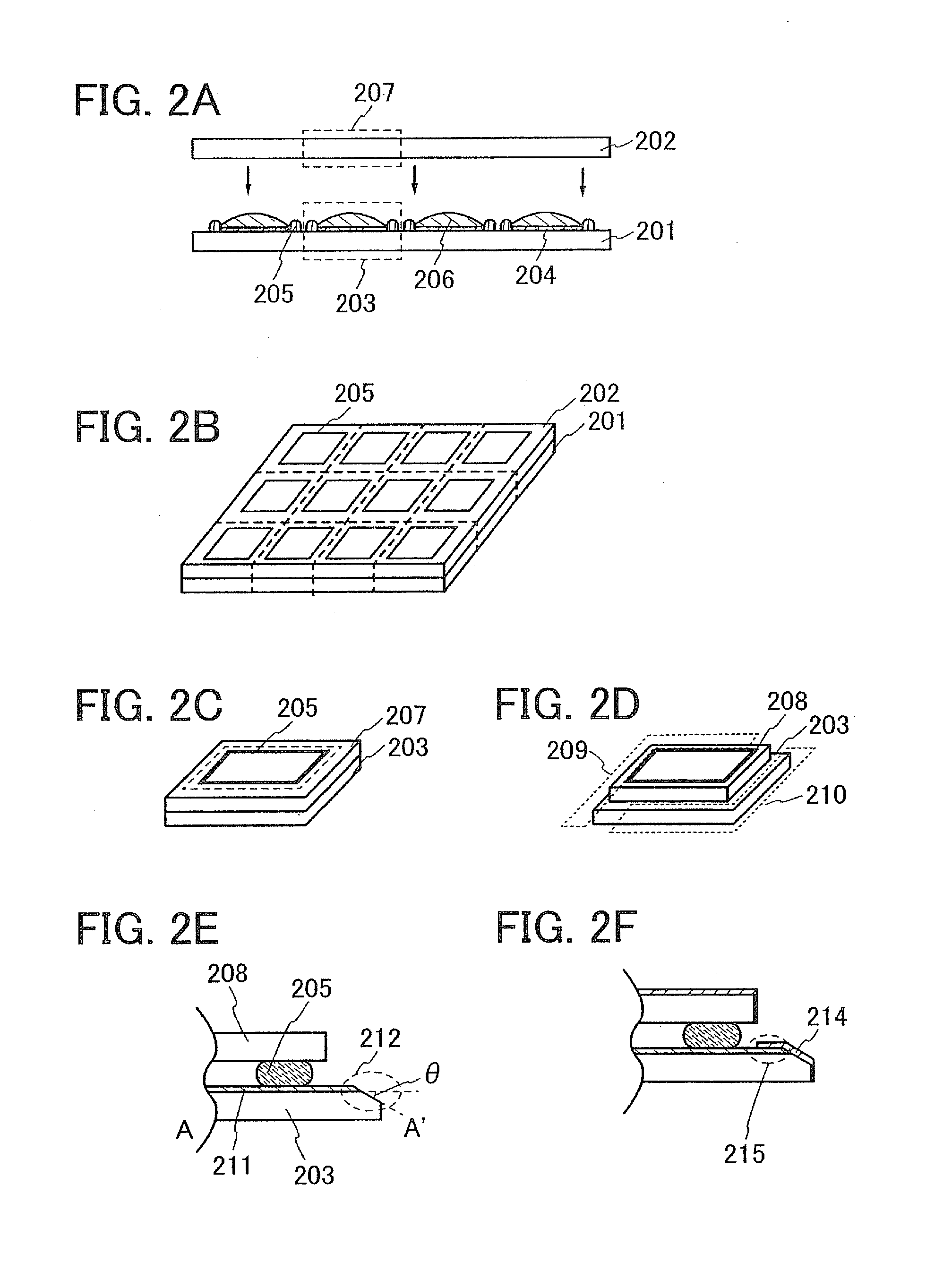
[0031]This embodiment mode will explain a liquid crystal panel used for a liquid crystal display device as an example of a display panel used for a display device. Specifically, a liquid crystal material is sandwiched between an active matrix substrate and an opposite substrate by a One Drop Filling (ODF) method. After attaching the both substrates, an element forming surface side of the end portion of the active matrix substrate is chamfered, a common wiring is formed in a chamfer portion or the like, and wirings (a source line, a gate line, a storage capacitor line, a leading out wiring, and the like) formed over the active matrix substrate are electrically connected by the common wiring. A case having such a structure will be explained. Note that the leading out wiring is an extracted portion of the source line, a gate line, the storage capacitor line, or the like, which is formed outside the pixel portion, and which connects the pixel portion and an external circuit.
[0032]FIG. 1...
embodiment mode 2
[0051]This embodiment mode will explain a liquid crystal panel used for a liquid crystal display device as an example of a display panel used for a display device. Specifically, after attaching an active matrix substrate, an element forming surface side of the end portion which is chamfered in advance, to an opposite substrate, a liquid crystal material is sandwiched between the both substrates, a common wiring is formed in a chamfer portion or the like, and wirings (a source line, a gate line, a storage capacitor line, a leading out wiring, and the like) formed over the active matrix substrate are electrically connected by the common wiring. A case having such a structure will be explained.
[0052]FIG. 4 shows a cross section of the end portion of a liquid crystal panel formed by being injected with a liquid crystal material 403 after attaching an active matrix substrate 401, which is chamfered in advance, and an opposite substrate 402 to each other with a sealant 404. Note that, alt...
embodiment mode 3
[0069]As the manufacturing method of the active matrix substrate that can be used for Embodiment Mode 1 or 2, this embodiment mode will particularly explain a manufacturing method of an amorphous silicon thin film transistor (TFT) and a pixel electrode formed in a pixel portion (reference numeral 204 of FIG. 3B and reference numeral 513 of FIGS. 6A and 6B) over an active matrix substrate, with reference to FIGS. 7A to 7E and FIGS. 8A to 8D. Note that explanation will be given in FIGS. 7A to 7E and FIGS. 8A to 8D with the common reference numerals.
[0070]As shown in FIG. 7A, a first conductive film 702 is formed over a substrate 701. The first conductive film 702 can be formed using a film formation method such as sputtering, PVD, CVD, droplet discharging, printing, or electroplating. As the material that is used to form the first conductive film 702, for example, a metal element such as Ag, Au, Cu, Ni, Pt, Pd, Ir, Rh, W, Al, Ta, Mo, Cd, Zn, Fe, Ti, Si, Ge, Zr, Ba, or Nd, an alloy mat...
PUM
| Property | Measurement | Unit |
|---|---|---|
| θ | aaaaa | aaaaa |
| θ | aaaaa | aaaaa |
| surface tension | aaaaa | aaaaa |
Abstract
Description
Claims
Application Information


