

Systems and methods for non-contact power and data transfer in electronic devices
a technology of non-contact power and data transfer, applied in the direction of transmission, circuit arrangement, inductance, etc., can solve the problems of increasing the complexity of the contact test system, additional testing, assembly and/or packaging, and the inability to fully function the entire devi
- Summary
- Abstract
- Description
- Claims
- Application Information
AI Technical Summary
Benefits of technology
Problems solved by technology
Method used
Image

Examples
Embodiment Construction
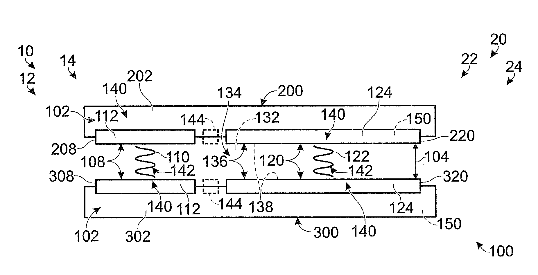
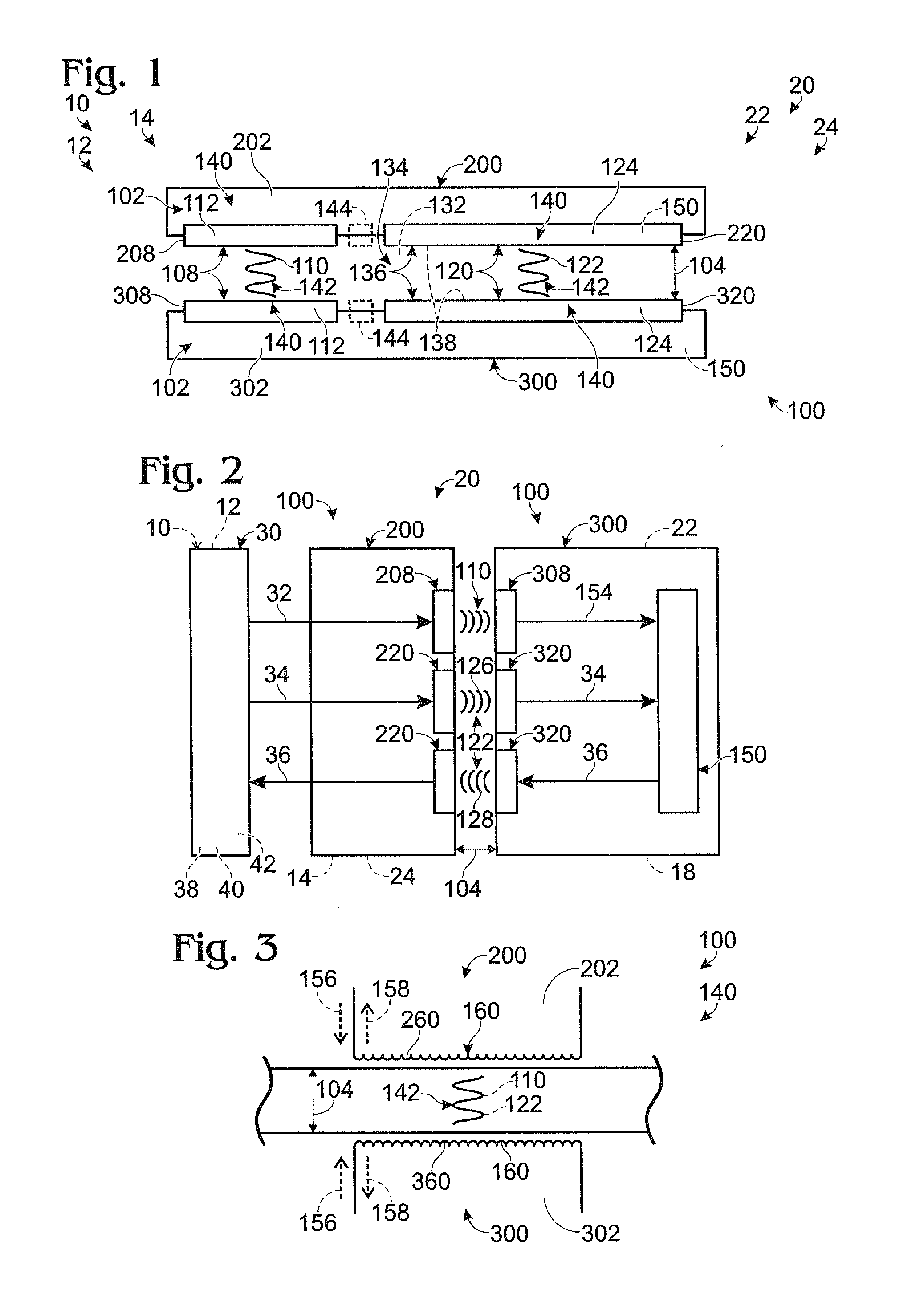
[0024]FIG. 1 is a schematic representation of illustrative, non-exclusive examples of electronic devices 100 according to the present disclosure. As discussed in more detail herein, electronic devices 100 may be included in, and / or form a portion of, a test system 10, which also may be referred to herein as a probe station. The test system may be configured to perform one or more test sequences, such as by providing one or more input data signals to a device under test and / or by receiving one or more resultant, or output, signals from the device under test. As illustrative, non-exclusive examples, electronic devices 100 may form a portion of a probe head 12 and / or a test tier 14 that may be in electrical communication with, and / or form a portion of, test system 10.
[0025]Additionally or alternatively, electronic devices 100 may he included in, and / or form a portion of, a three-dimensional (3-D) integrated circuit 20, which may be utilized in any suitable electronic device. As an illu...
PUM
 Abstract
Description
Claims
Application Information