Photodiode employing surface grating to enhance sensitivity

Active Publication Date: 2013-08-15
TEXAS INSTR INC
View PDF6 Cites 8 Cited by
  • Summary
  • Abstract
  • Description
  • Claims
  • Application Information

AI Technical Summary

Benefits of technology

[0004]The following presents a simplified summary in order to provide a basic understanding of one or more aspects of the invention. This summary is not an extensive overview of the invention, and is neither intended to identify key or critic

Problems solved by technology

A portion of the incident light may be undesirably lost at the top surface, due to reflection.
Dielectric antireflection layers such as magne

Method used


Image

  • Photodiode employing surface grating to enhance sensitivity
  • Photodiode employing surface grating to enhance sensitivity
  • Photodiode employing surface grating to enhance sensitivity

Examples


Embodiment Construction

[0008]The following applications contains related materials and are hereby incorporated in their entirety: Application ______ (TI-71977PS) entitled “LOW-CAPACITANCE PHOTODIODE UTILIZING VERTICAL CARRIER CONFINEMENT” and Application ______ (TI-71978PS) entitled “WAVELENGTH SENSITIVE PHOTODIODE EMPLOYING SHORTED JUNCTION” filed concurrently with this application.

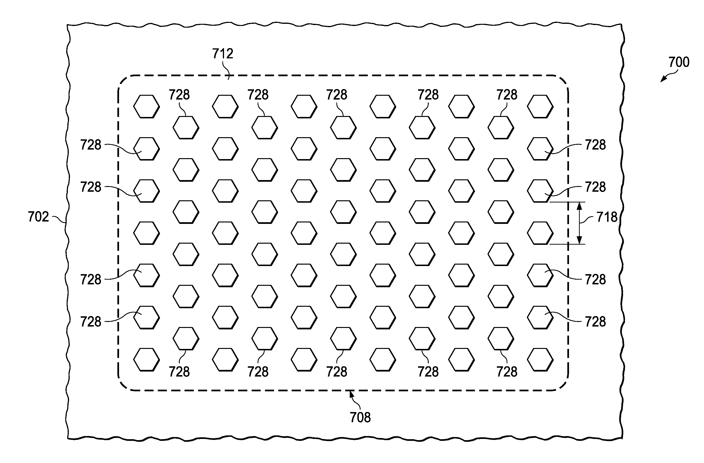
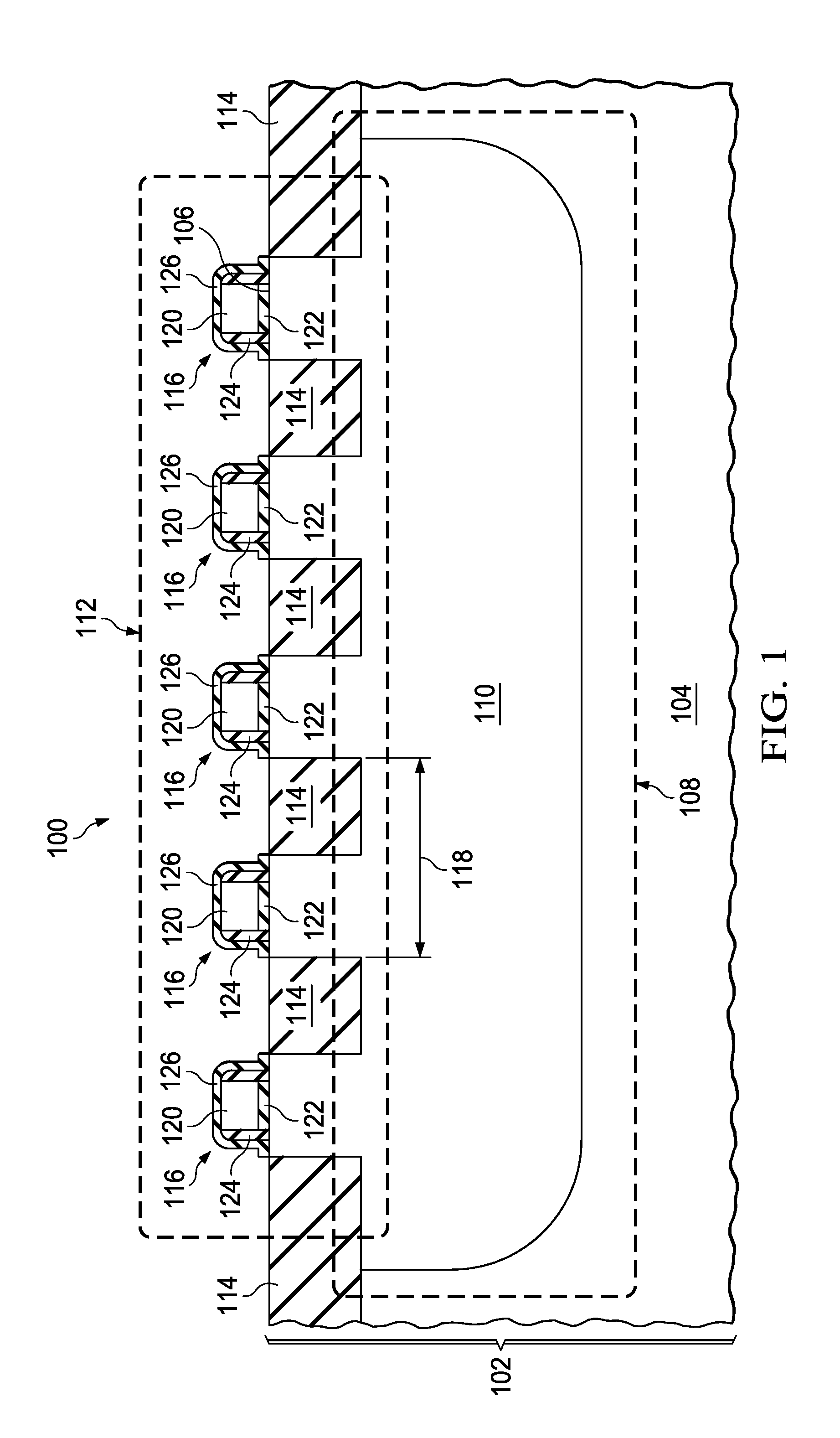
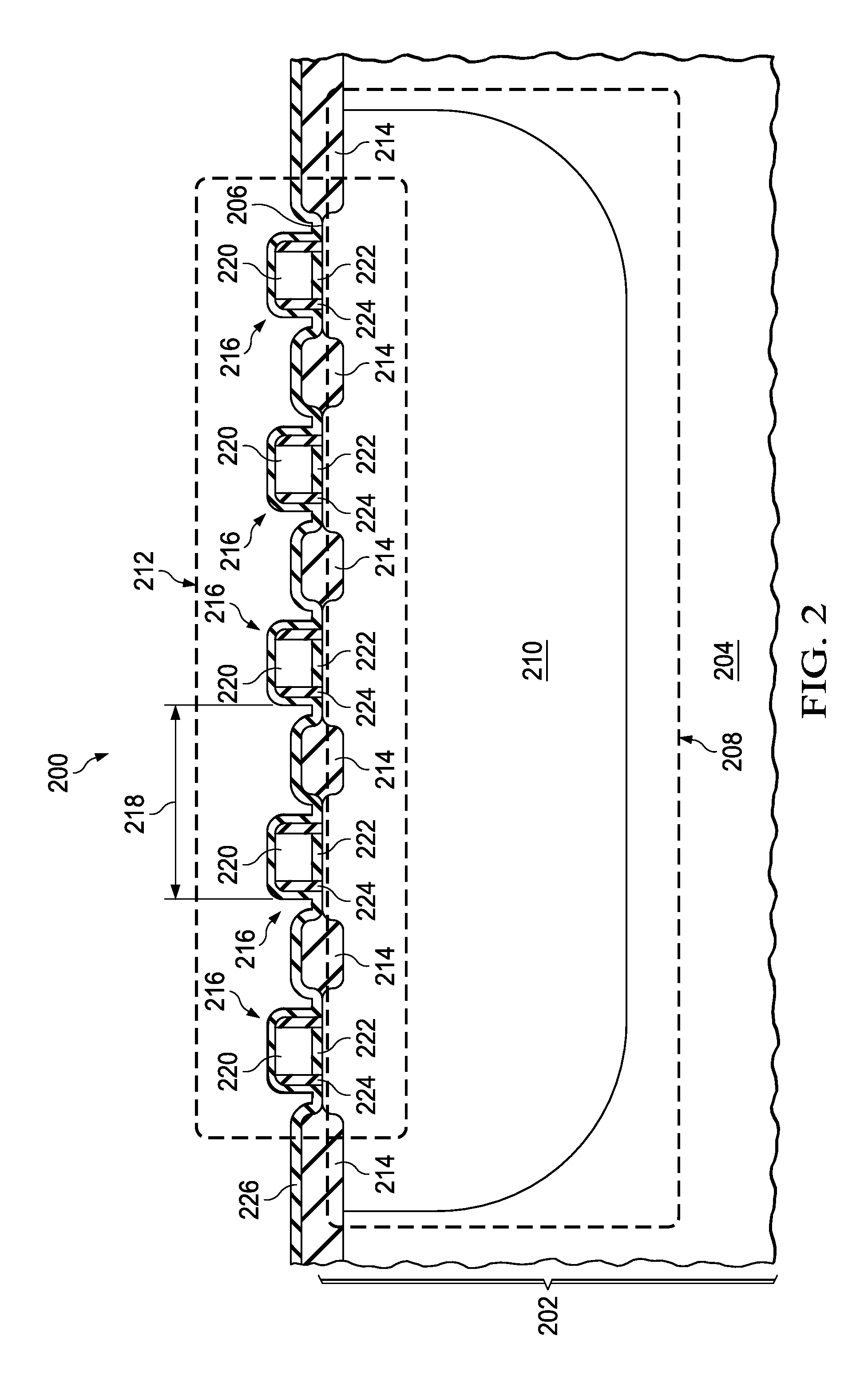
[0009]The present invention is described with reference to the attached figures. The figures are not drawn to scale and they are provided merely to illustrate the invention. Several aspects of the invention are described below with reference to example applications for illustration. It should be understood that numerous specific details, relationships, and methods are set forth to provide an understanding of the invention. One skilled in the relevant art, however, will readily recognize that the invention can be practiced without one or more of the specific details or with other methods. In other instances, well-known structur...


PUM


Abstract

A semiconductor device contains a photodiode formed in a substrate of the semiconductor device. At a top surface of the substrate, over the photodiode, a surface grating of periodic field oxide in a periodic configuration and/or gate structures in a periodic configuration is formed. The field oxide may be formed using an STI process or a LOCOS process. A semiconductor device with a surface grating including both field oxide and gate structures has the gate structures over the semiconductor substrate, between the field oxide. The surface grating has a pitch length up to 3 microns. The surface grating covers at least half of the photodiode.

Description

CROSS-REFERENCE TO RELATED APPLICATIONS[0001]This application claims the benefit of priority under U.S.C. §119(e) of U.S. Provisional Application 61 / 599,299 (TI-71979PS), filed Feb. 15, 2012.FIELD OF THE INVENTION[0002]This invention relates to the field of semiconductor devices. More particularly, this invention relates to photodiodes in semiconductor devices.BACKGROUND OF THE INVENTION[0003]A photodiode in a semiconductor device may receive incident light through a top surface of the semiconductor device and covert the light into a signal current. A portion of the incident light may be undesirably lost at the top surface, due to reflection. Dielectric antireflection layers such as magnesium fluoride may be deposited on the top surface, but may undesirably increase fabrication cost and complexity of the semiconductor device.SUMMARY OF THE INVENTION[0004]The following presents a simplified summary in order to provide a basic understanding of one or more aspects of the invention. Thi...

Claims


Application Information

Patent Timeline
IPC IPC(8): H01L31/0236
CPCH01L31/02366H01L31/103H01L31/02327H01L31/02161
Inventor EDWARDS, HENRY LITZMANNTRIFONOV, DIMITAR TRIFONOV
Owner TEXAS INSTR INC
Why Eureka
Try Eureka