

Generation of a frequency comb and applications thereof
a frequency comb and frequency technology, applied in the field of measuring the properties of semiconductors, can solve the problems of increasing noise, difficult fabrication, and presently a lower resolution limit of 10 nm, and achieve the effect of improving the accuracy at which the dopant concentration of a depletion region is measured
- Summary
- Abstract
- Description
- Claims
- Application Information
AI Technical Summary
Benefits of technology
Problems solved by technology
Method used
Image

Examples
example
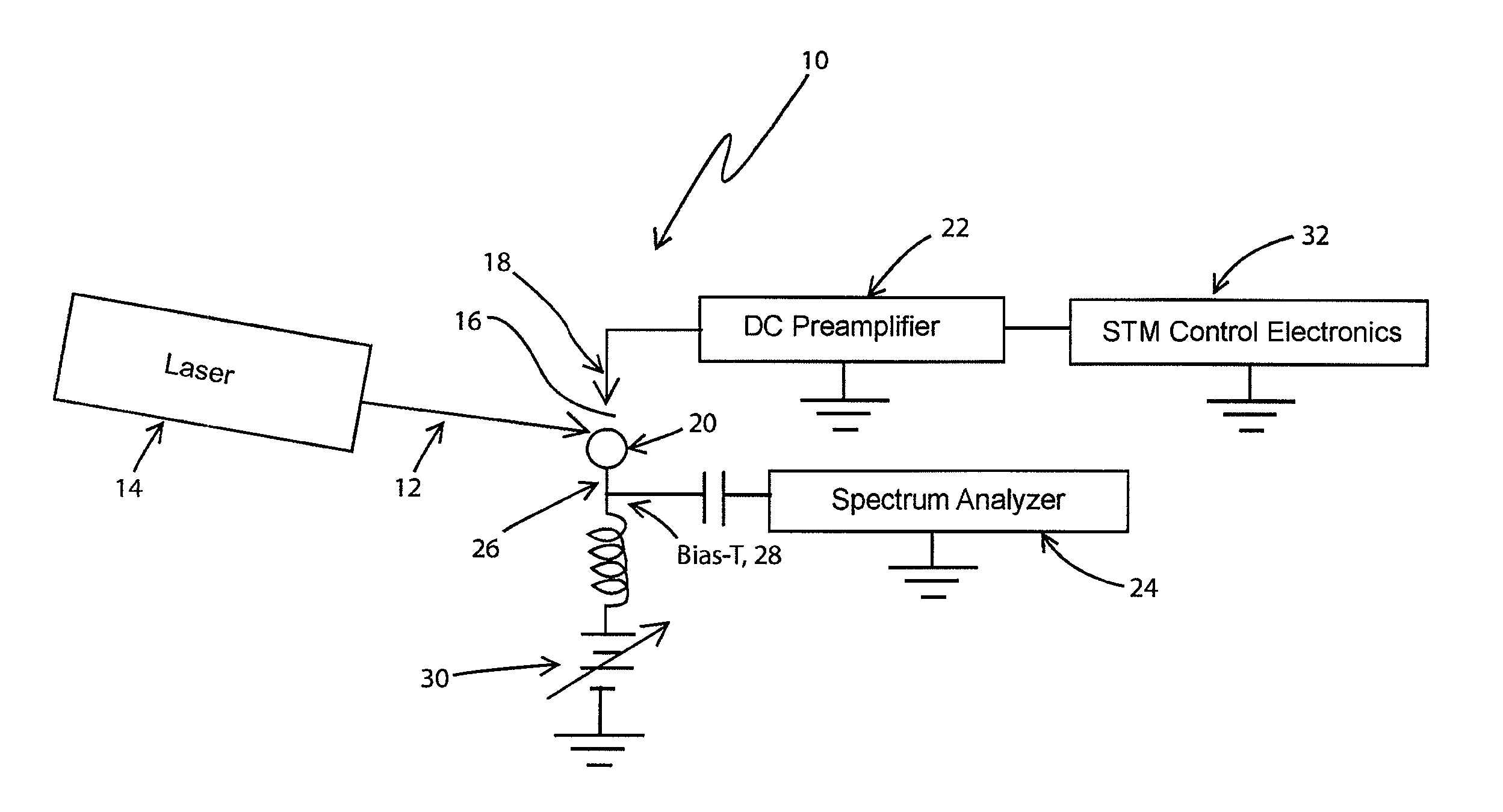
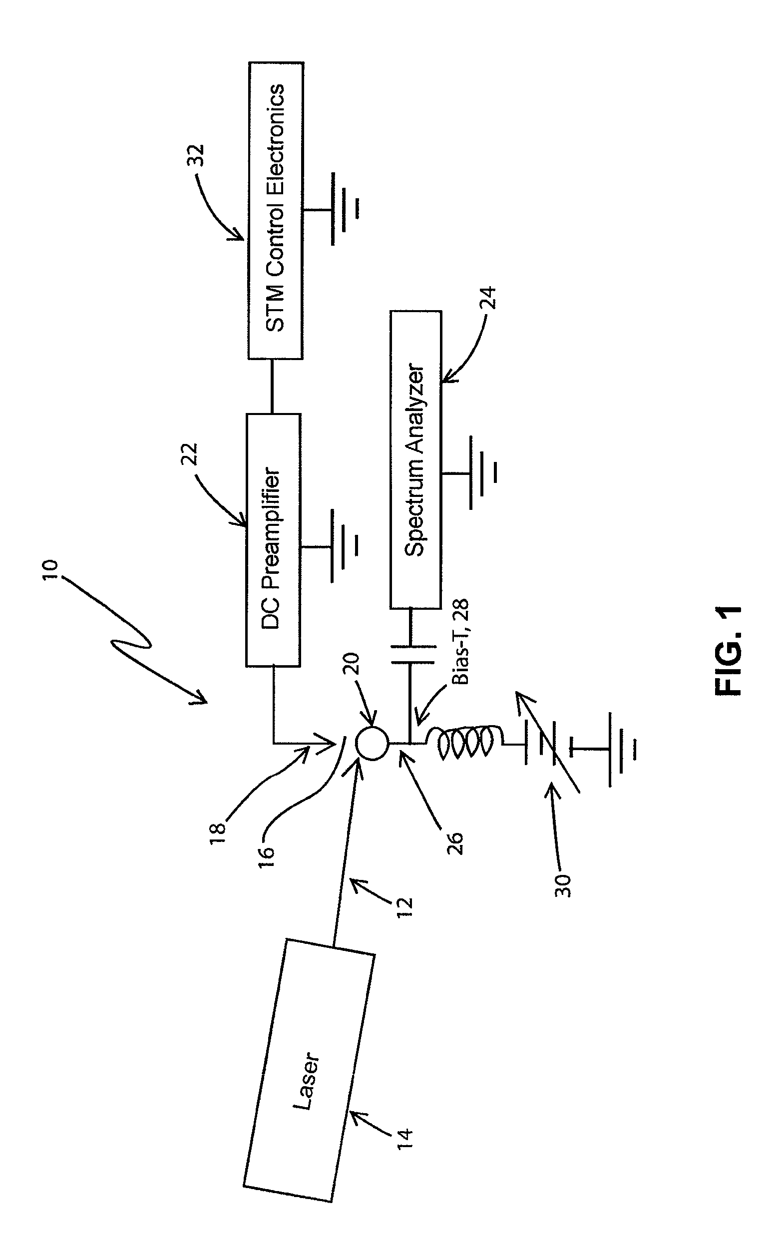
[0039]In the following EXAMPLE, the microwave frequency comb is used measure the nanoscale dopant profile of semiconductors:
[0040]A negative or positive DC bias voltage applied to the tip electrode of a STM causes a depletion layer at the surface of an n-type or p-type semiconductor sample, respectively. In what follows, n-type semiconductors will be described, but the application to p-type semiconductors is straight forward to one having skill in the semiconductor art.
[0041]The close proximity of tip 18 to semiconductor sample 20 causes depletion layer, 34, to have an approximately hemispherical shape as shown in FIG. 6. As the DC bias is made more negative, radius, 36, of the depletion layer increases, as a function of the density of major carriers at outer surface, 38, of the hemisphere. Thus, if the capacitance of the depletion layer is determined as a function of the applied DC bias, the average density of major carriers at each hemispherical surface may be calculated, from whi...
PUM
 Abstract
Description
Claims
Application Information