Magnetoresistive logic cell and method of use

a logic cell and magnetoresistive technology, applied in static storage, digital storage, instruments, etc., to achieve the effect of reducing the mtj junction of the ra product, high resistance state of the mrlc, and effective capacitan

Active Publication Date: 2013-08-22
AVALANCHE TECH
View PDF2 Cites 6 Cited by
  • Summary
  • Abstract
  • Description
  • Claims
  • Application Information

AI Technical Summary

Benefits of technology

[0017]The relative magnetization orientations of the common free layer and the switchable reference layer in MTJ-1 dominate the overall resistance of the MRLC without regard to the fixed magnetization orientation of the nonswitchable reference layer in MTJ-2 which makes only a small contribution. This behavior is different from that of a standard MTJ in which the resistance is determined by the relative orientations of the free layer and the pinned layer. The high resistance state of the MRLC occurs when the switchable reference and common free layers have opposite magnetization orientations. The low resistance state occurs when the reference layer and free layer have the same magnetization orientation. This behavior allows the MRLC to be used as a logical comparator.
[0018]An MRLC according to the invention has MTJ-2 designed to have a substantially lower RA product MTJ junction than MTJ-1. MTJ-1 has an effective capacitance that is much larger than that of MTJ-2. Embodiments of the invention allow the CFL to be switched with reference to the nonswitchable reference layer by STT effect through application of selected relatively short voltage pulses that do not switch the SRL. The SRL can be switched with reference to the CFL by a voltage effect generated by a selected longer voltage pulse that does not switch the CFL.
[0019]The pulses used for setting the CFL have a different set of characteristics including shape and duration than the pulses used to set the SRL. In embodiments pulses for setting the CFL can be relatively square (fast rise time) and short duration, while pulses for setting the SRL are preferably ramped (slow rise time) and relatively long in duration. Positive and negative voltage polarity are used to set the CFL magnetization direction. A voltage-induced switching principle can be used with MRLC embodiments of the present invention to switch the SRL to parallel or anti-parallel with respect to the magnetization of the CFL in both perpendicular and in-plane anisotropy embodiments. The benefit is that the SRL can be selectively switched in either anti-parallel and parallel directions in relation to the CFL depending on the applied voltage amplitude, while voltage polarity of the pulses does not change.
[0020]The different methods of setting the common free layer (CFL) and the switchable reference layer (SRL) allow the SRL to serve as a long term data storage layer while the CFL serves for short term data storage. This allows a single MRLC device to serve as a fully functional logic cell, which usually requires a much more complicated and bulky circuitry when formed entirely by conventional CMOS circuits.

Problems solved by technology

However, due to this low RA and high current density, when a voltage is applied to the MTJ, charges (accumulated and depleted electrons) will not be held within the magnetic layers adjacent to the barrier layer to provide a capacitive effect.

Method used


Image

  • Magnetoresistive logic cell and method of use
  • Magnetoresistive logic cell and method of use
  • Magnetoresistive logic cell and method of use

Examples


embodiment # 2 (illustrated in fig.8)

MRLC Embodiment #2 (Illustrated in FIG. 8)

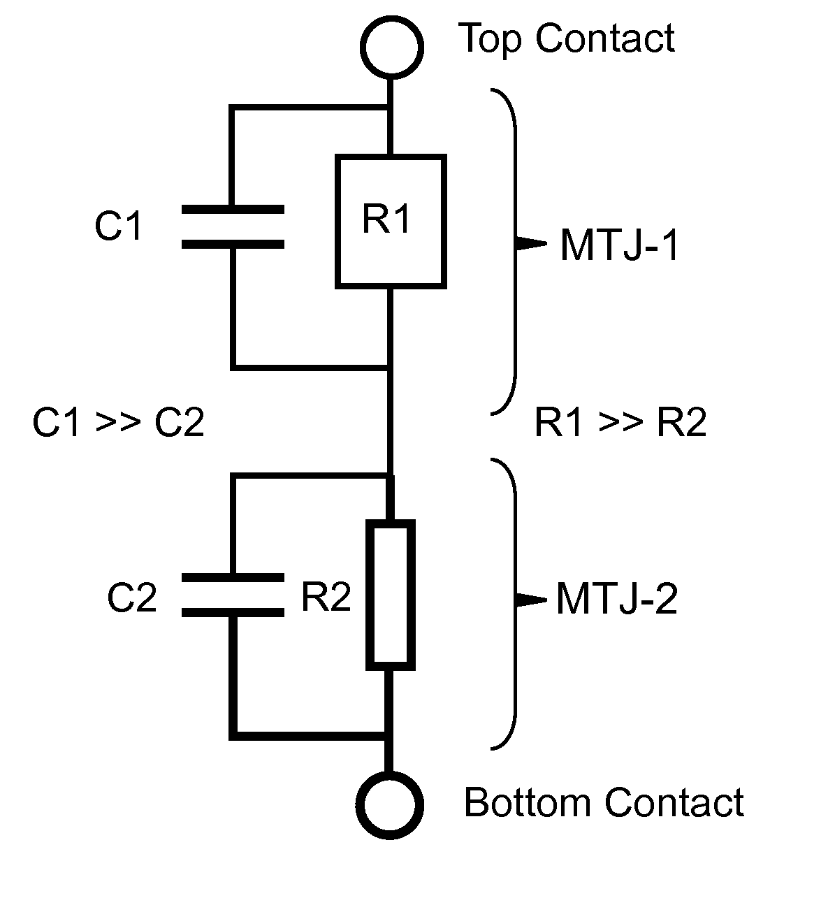
[0101]A second example of an magnetoresistive logic cell (MRLC) 50A device with a layer structure as shown in FIG. 8 will now be described. In this embodiment two additional layers are added to the structure of embodiment #1 and except for these additional layers the description above for embodiment #1 applies. As noted for embodiment #1 the entire structure can be flipped upside down as an alternative embodiment. In embodiment #2, anti-ferromagnetic exchange coupling layer 56P and magnetic pinned layer 57P are added below the nonswitchable reference layer (NRL) 55P. Embodiment #2 has an advantage over embodiment #1 because the additional magnetic field component generated by pinned layer 57P partially cancels out the magnetic field component from NRL 55P acting on common free layer 51P and switchable reference layer 53P. This reduces static coupling on the switchable layers 51P and 53P so that switching is less biased than in embodiment #1....

embodiment # 3 (illustrated in fig.9)

MRLC Embodiment #3 (Illustrated in FIG. 9)

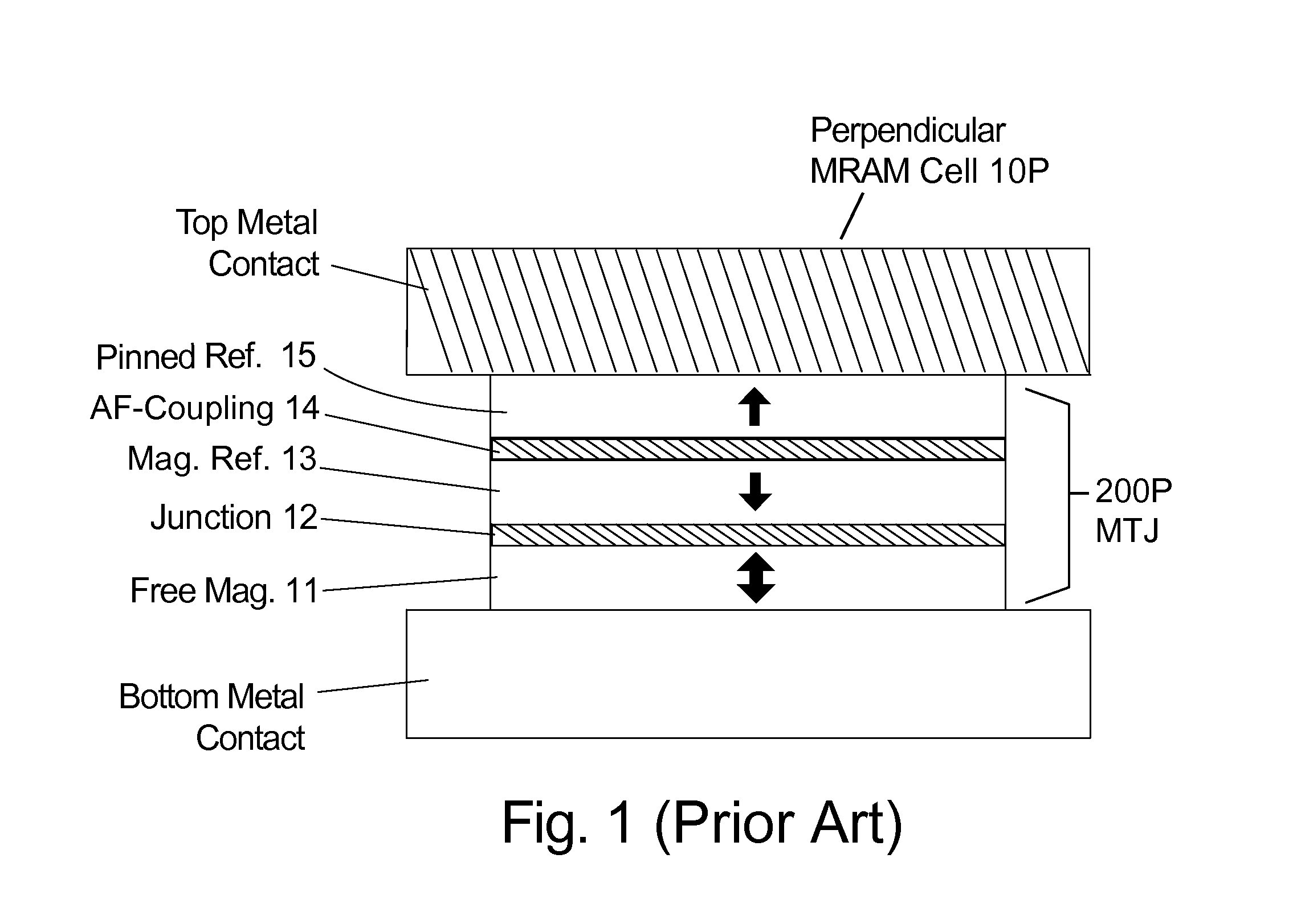
[0104]A third example of a magnetoresistive logic cell (MRLC) 50B with a layer structure as shown in FIG. 9 will now be described. In this embodiment all of the magnetic layers have easy magnetization axes in the film plane, i.e. in-plane anisotropy. As for the previous embodiments, the entire layer structure can be flipped upside down as an alternative embodiment. Current flow is between the top and bottom contacts.

[0105]In embodiment #3, the function of the nonswitchable reference layer 55H is enhanced by adding anti-ferromagnetic (AF) exchange coupling layer 56H, magnetic pinned layer 57H, and anti-ferromagnetic layer 58H between nonswitchable reference layer 55H and the bottom contact. This 4-layer structure forms a generic reference & pinned layer structure which is known in the art for use in MRAM in-plane MTJs. The advantages for using this 4-layer structure in a conventional single MTJ MRAM device also apply to use in an in-plane MRL...


PUM


Abstract

A magnetoresistive logic cell (MRLC) is described that includes two MTJs in series that share a common free layer (CFL). The relative magnetization orientations of the CFL and the switchable reference layer (SRL) in MTJ-1 dominate the overall resistance of the MRLC without regard to the fixed magnetization orientation of the nonswitchable reference layer in MTJ-2. High and low resistance states of the MRLC occurs based on the relative magnetization orientations of SRL and CFL. This behavior allows the MRLC to be used as a logical comparator. The CFL is switched by STT effect by application of selected relatively short voltage pulses that do not switch the SRL. A voltage-induced switching principle can be used with MRLC embodiments of the present invention to switch the SRL to parallel or anti-parallel with respect to the magnetization CFL in both perpendicular and in-plane anisotropy embodiments.

Description

CROSS REFERENCE TO RELATED APPLICATIONS[0001]This application is a Continuation-In-Part of co-pending U.S. patent application bearing Ser. No. 13 / 402,123 with filing date of Feb. 22, 2012, and entitled “MAGNETORESISTIVE LOGIC CELL AND METHOD OF USE” which is hereby incorporated by reference.FIELD OF THE INVENTION[0002]The present invention relates to the design and use of magnetoresistive random access memory (MRAM) cells that include magnetic tunnel junctions (MTJ) memory elements.BACKGROUND OF THE INVENTION[0003]FIG. 1 illustrates an MRAM cell 10P with MTJ 200P in which the easy axes of the magnetic layers are perpendicular to the plane of the thin films as illustrated by the arrows on the magnetic layers 15, 13, 11. MTJs can also be designed with in-plane magnetization. An MRAM cell structure typically includes a top metal contact and a bottom metal contact. The metal contacts are also referred to as electrodes.[0004]A typical STT-MRAM (spin transfer torque magnetic random access...

Claims


Application Information

Patent Timeline
Patent Type & Authority Applications(United States)
IPC IPC(8): G11C11/16
CPCG11C11/161G11C11/16Y10S977/935Y10S977/933G11C11/1675
Inventor ZHOU, YUCHENWANG, ZIHUIHUAI, YIMING
Owner AVALANCHE TECH
Why Eureka
Try Eureka