
Light emitting element and production method for same, production method for light-emitting device, illumination device, backlight, display device, and diode

Active Publication Date: 2013-08-29
ELUX INC
View PDF12 Cites 43 Cited by
  • Summary
  • Abstract
  • Description
  • Claims
  • Application Information

AI Technical Summary

Benefits of technology

The invention relates to a diode that can provide desired properties to its core without increasing manufacturing costs or decreasing production yield. This is achieved by fulfilling the roles of two poles of the diode using two semiconductor layers. By selecting a desired material for the core part, its properties (such as refractive index, thermal conductivity or electrical conductivity) can be optimally matched.

Problems solved by technology

Thus there has been a problem in that the increase in the length of the rods involves increase in length of the highly resistant active layer, causes decrease in brightness of extremity parts thereof because of failure to pass a sufficient current to the extremity parts, and hinders obtainment of a sufficient emission intensity.

Method used


Image

  • Light emitting element and production method for same, production method for light-emitting device, illumination device, backlight, display device, and diode
  • Light emitting element and production method for same, production method for light-emitting device, illumination device, backlight, display device, and diode
  • Light emitting element and production method for same, production method for light-emitting device, illumination device, backlight, display device, and diode

Examples


first embodiment

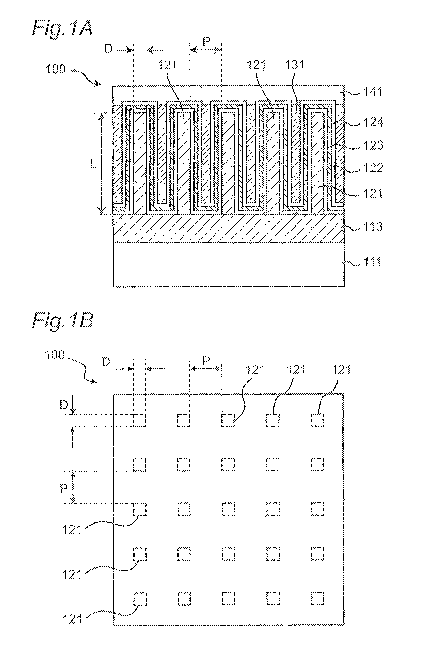
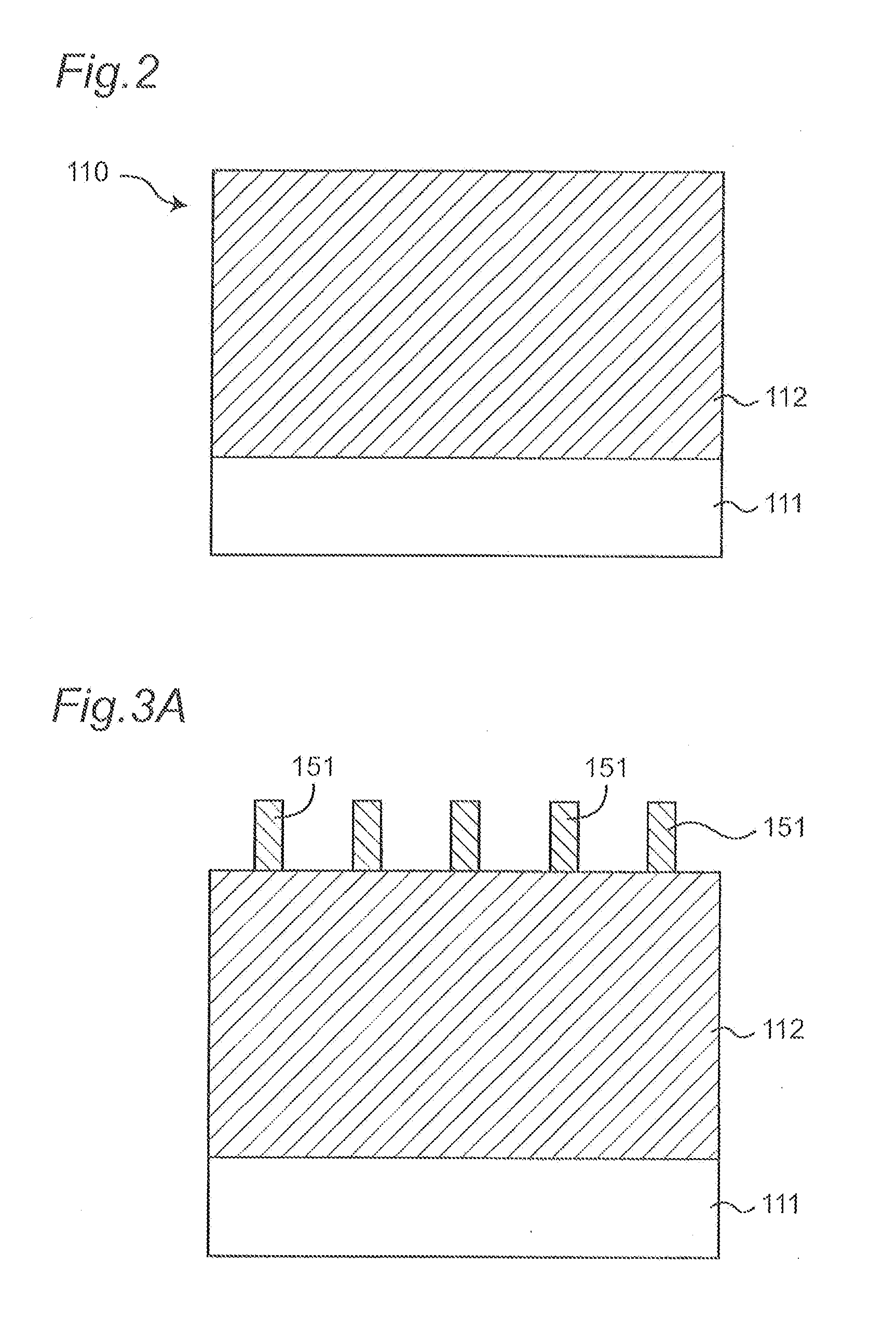
[0189]A light-emitting element according to a first embodiment of the invention will be described with reference to FIGS. 1A, 1B, and 2 through 6. FIG. 1A is a sectional view of the light-emitting element of the first embodiment. FIG. 1B is a view of the light-emitting element of the first embodiment as seen looking from above, the view exclusively showing positions of rod-shaped semiconductors. FIGS. 2 through 6 are diagrams for illustrating a production method for the light-emitting element of the first embodiment. The light-emitting element 100 of the first embodiment has an n-type semiconductor layer 113 as a first conductivity type semiconductor base, a plurality of n-type rod-shaped semiconductors 121 formed on the n-type semiconductor layer 113, and a p-type semiconductor layer 123, as a second conductivity type semiconductor layer, covering the rod-shaped (protrusion-shaped) semiconductors 121. As the first conductivity type semiconductor base, a p-type semiconductor layer m...

second embodiment

[0222]Next, a second embodiment of a light-emitting element of the invention will be described with reference to FIGS. 7A through 7C. FIG. 7A is a sectional view of the light-emitting element of the second embodiment. FIG. 7B is a plan view of the light-emitting element of the second embodiment as seen looking from above, the plan view exclusively showing positions of plate-like semiconductors. FIG. 7C is a plan view for illustrating a production method for the light-emitting element of the second embodiment.

[0223]The light-emitting element 1100 of the second embodiment is different from the first embodiment in that the plate-like semiconductors 1121 are provided in place of the plurality of rod-shaped (protrusion-shaped) semiconductors 121 of the first conductivity type (n-type) in the light-emitting element 100 of the first embodiment. For the second embodiment, therefore, description will be omitted on details of parts thereof common to those of the first embodiment.

[0224]In FIGS...

third embodiment

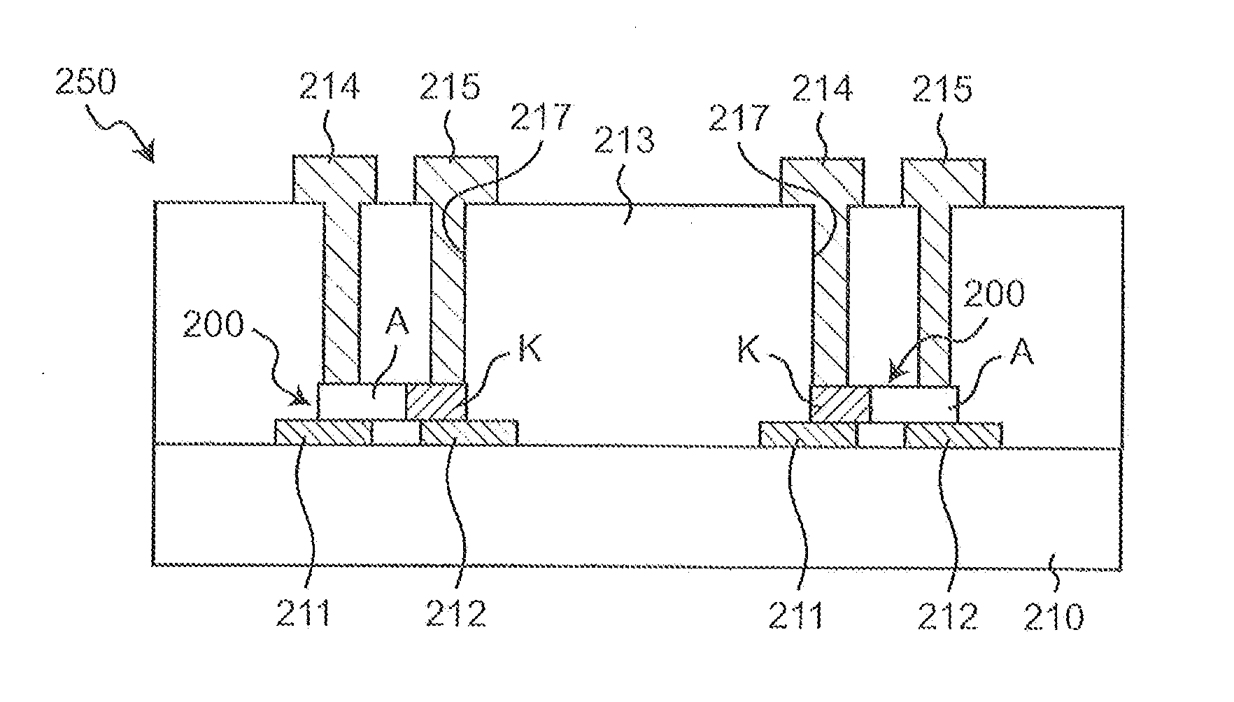
[0240]Next, a production method for light-emitting elements and a light-emitting device as a third embodiment of the invention will be described with reference to FIGS. 8 through 17. FIGS. 8 through 17 are diagrams showing steps of forming the light-emitting elements and the light-emitting device in the third embodiment.

[0241]Process steps in former half of the production method of the third embodiment are the same as the steps for production of the first embodiment that have been described with reference to FIGS. 2 through 5. Therefore, duplicate description on the steps for production of FIGS. 2 through 5 for the first embodiment is omitted here and steps subsequent to the steps of FIGS. 2 through 5 will be described. Alternatively, in the steps in the former half in the production method of the third embodiment, the step described with reference to FIG. 3A in the first embodiment may be replaced by the step described with reference to FIG. 7C for the second embodiment, so that th...


PUM


Abstract

A light-emitting element includes a first conductivity type semiconductor base, a plurality of first conductivity type protrusion-shaped semiconductors formed on the semiconductor base, and a second conductivity type semiconductor layer that covers the protrusion-shaped semiconductors.

Description

REFERENCE TO RELATED APPLICATIONS[0001]This application is a national stage application under 35 USC 371 of International Application N PCT / JP2011 / 064231, filed Jun. 22, 2011, which claims the priority of Japanese Patent Application Nos. 2010-195788, filed Sep. 1, 2010, 2010-208023, filed Sep. 16, 2010, and 2011-122176, filed May 31, 2011, the entire contents of which are incorporated herein by reference.FIELD OF THE INVENTION[0002]The present invention relates to light-emitting elements having protrusion-shaped semiconductors shaped like rods, plates or the like and a production method for the same, a production method for a light-emitting device having such light-emitting elements, an illumination device, a backlight and a display device each of which has such a light-emitting device, and to a diode constituting a light-emitting diode, a photoelectric conversion element or the like.BACKGROUND OF THE INVENTION[0003]A conventional rod-type light-emitting element having a light-emitt...

Claims


Application Information

Patent Timeline
IPC IPC(8): H01L33/64H01L33/58H01L33/08H01L33/42
CPCH01L33/64Y02E10/52H01L33/58H01L33/08G02F1/133603H01L25/0753H01L33/0079H01L33/18H01L33/20H01L33/24H01L33/32H01L31/035227H01L31/03529H01L2924/0002H01L33/42H01L31/0547H01L2924/00H01L31/054H01L33/14H01L33/26H01L33/0093H01L33/04H01L33/22H01L31/052
Inventor SHIBATA, AKIHIDENEGISHI, TETSUKOMIYA, KENJIYAOI, YOSHIFUMISHIOMI, TAKESHIIWATA, HIROSHITAKAHASHI, AKIRA
Owner ELUX INC
Learn More